Component arrangement and method for producing a component arrangement

a technology of component arrangement and component assembly, which is applied in the direction of beam/ray focussing/reflecting arrangement, biochemistry apparatus and processes, instruments, etc., can solve the problems of complicated metallizing of conductor tracks, restricting the layout of conductor tracks, and requiring the application of conductor tracks or flow stops

Active Publication Date: 2015-02-17
DR JOHANNES HEIDENHAIN GMBH
View PDF17 Cites 1 Cited by
  • Summary
  • Abstract
  • Description
  • Claims
  • Application Information

AI Technical Summary

Benefits of technology

The present invention provides a component assembly and method for making it that prevents unwanted material from flowing during encapsulation. This is achieved by using a flow stop bonding wire that defines a boundary zone between the semiconductor component and the encapsulation. Other flow stop bonding wires may also be used at different locations on the carrier element. The flow stop bonding wire is fixed on its ends, and its arrangement parallel to the semiconductor component and oriented towards the encapsulation is advantageous. The technical effect is that this invention allows for reliable and controlled material flow during encapsulation, without requiring major additional process technology.

Problems solved by technology

However, this causes restrictions in the layout of the conductor tracks on the carrier element if the conductor tracks must additionally function as a flow stop.
Moreover, applying the conductor tracks or flow stop requires complicated metallizing via a masking process.

Method used


Image

  • Component arrangement and method for producing a component arrangement
  • Component arrangement and method for producing a component arrangement
  • Component arrangement and method for producing a component arrangement

Examples


Embodiment Construction

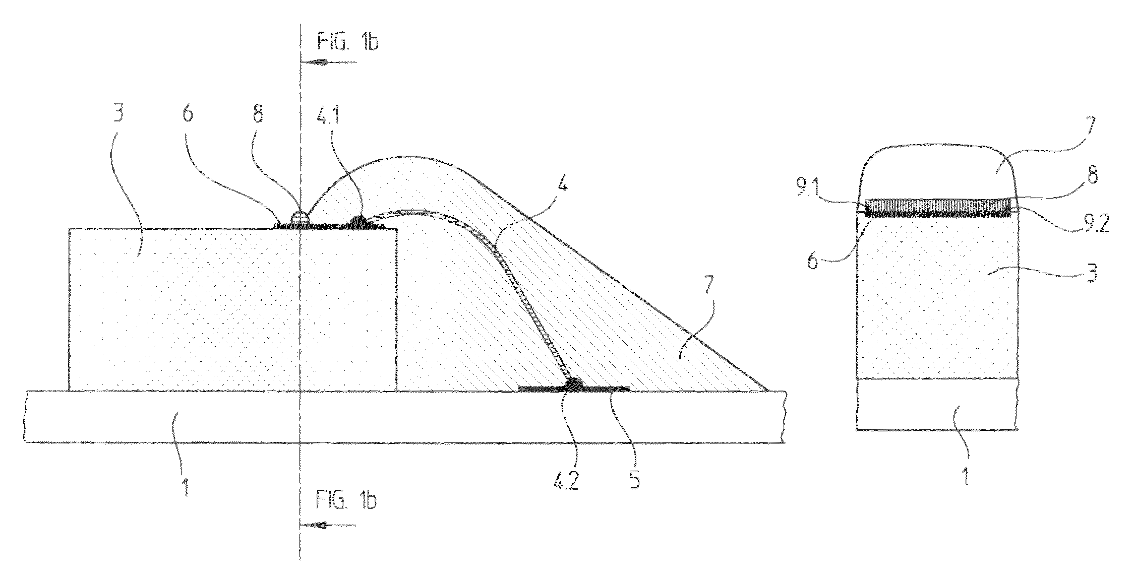
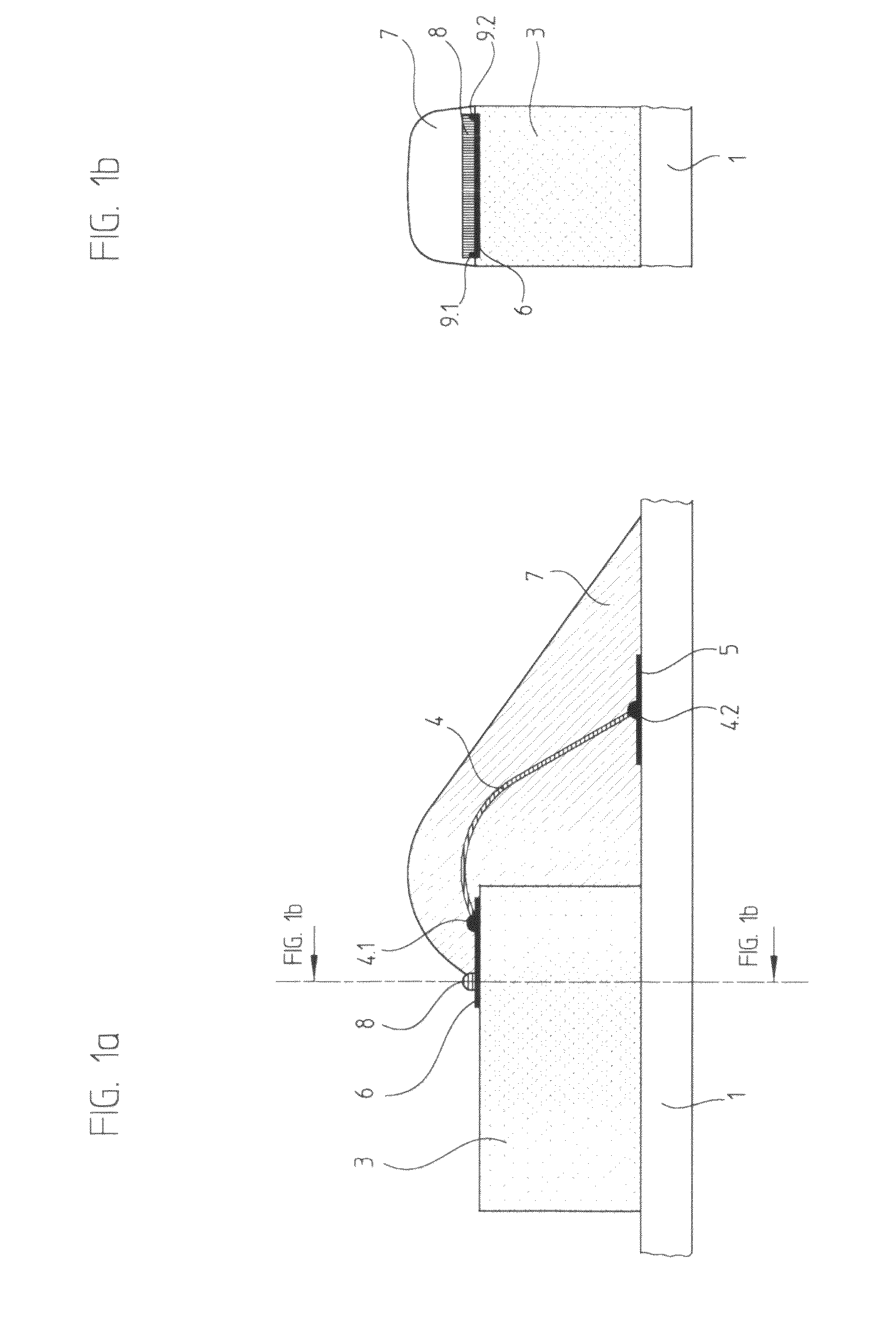
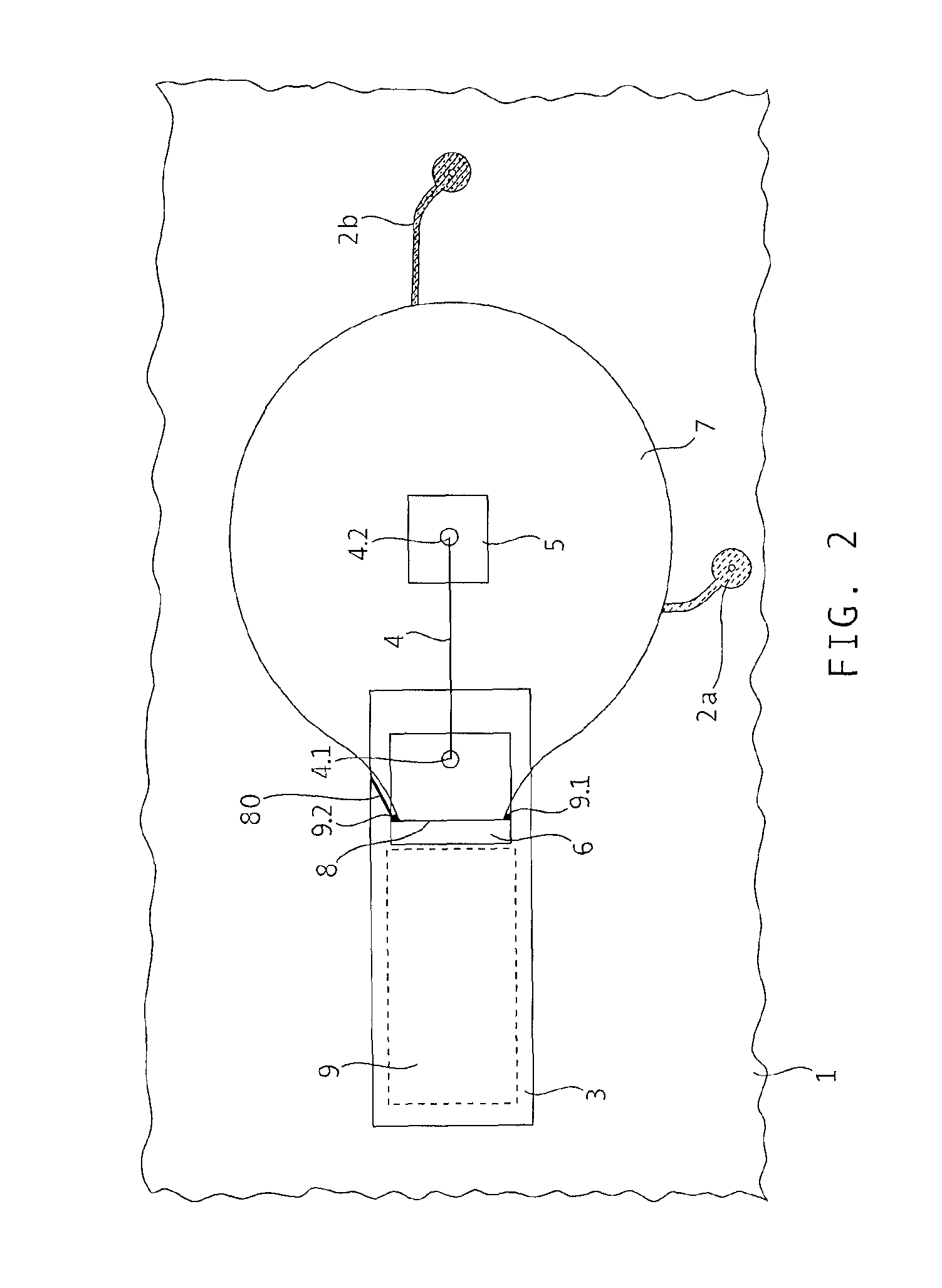
[0038]In FIGS. 1a and 1b, sectional views of a first embodiment of the component assembly of the invention are shown. FIG. 2 shows a top view on this exemplary embodiment. A first variant of the component assembly of the present invention will be described below in conjunction with these Figures.

[0039]The further components, to be described below, of the component assembly of the present invention are disposed on a carrier element 1. The carrier element 1 in this example is embodied as a known printed circuit board of FR4 material. Alternatively, other materials can be considered for the carrier element 1, such as ceramic or flexible circuit board material, and so forth.

[0040]As shown in FIG. 2, metal conductor tracks 2a, 2b are disposed in or on the carrier element 1 and serve to make electrical contact for the semiconductor component 3, disposed on the carrier element 1, and possibly for further components. As the semiconductor component 3, in the exemplary embodiment shown, an un...


PUM

PropertyMeasurementUnit
angleaaaaaaaaaa
heightaaaaaaaaaa
heightaaaaaaaaaa

Abstract

A component assembly including a carrier element including a first contact face and a semiconductor component disposed on the carrier element, wherein the semiconductor component includes a second contact face. The component assembly further includes a contact-making bonding wire, wherein one end of the contact-making bonding wire is connected to the first contact face and a second end of the contact-making bonding wire is connected to the second contact face. The component assembly includes a flow stop bonding wire positioned on the second contact face, wherein the flow stop bonding wire defines on the second contact face a first zone and a second zone. An encapsulation material is applied from the first zone to the first contact face so as to define an encapsulation for the flow stop bonding wire, wherein the flow stop bonding wire prevents an uncontrolled flow of the encapsulation material into the second zone.

Description

[0001]Applicant claims, under 35 U.S.C. §§120 and 365, the benefit of priority of the filing date of Mar. 3, 2009 of a Patent Cooperation Treaty patent application, copy attached, Serial Number PCT / EP2009 / 052497, filed on the aforementioned date, the entire contents of which are incorporated herein by reference, wherein Patent Cooperation Treaty patent application Serial Number PCT / EP2009 / 052497 was not published under PCT Article 21(2) in English.[0002]Applicant claims, under 35 U.S.C. §119, the benefit of priority of the filing date of Apr. 3, 2008 of a German patent application, copy attached, Serial Number 10 2008 017 012.7, filed on the aforementioned date, the entire contents of which are incorporated herein by reference.BACKGROUND OF THE INVENTION[0003]1. Field of the Invention[0004]The present invention relates to a component assembly and to a method for producing a component assembly.[0005]2. Description of the Related Art[0006]An optoelectronic component assembly is known ...

Claims


Application Information

Patent Timeline
Patent Type & Authority Patents(United States)
IPC IPC(8): H01L31/0203H01L23/00H01L23/24H01L23/31
CPCH01L23/24H01L23/3121H01L24/48H01L23/3185H01L2924/01033H01L24/45H01L2224/48091H01L2224/48227H01L2924/01082H01L2924/01013H01L2924/01006H01L2224/48464H01L2224/45124H01L2224/48699H01L2924/01079H01L2224/8592H01L2924/014H01L2924/01005H01L2224/45015H01L2924/00014H01L2924/00H01L2224/85399H01L2224/05599
Inventor ANGERER, ROMAN
Owner DR JOHANNES HEIDENHAIN GMBH
Why Eureka
Try Eureka