Mask design method, program, and mask design system

a mask design and mask technology, applied in the field of mask design technology, can solve the problems of limiting optimization performance, rule-based topology modification technology becoming less effective in the fabrication of state of the art semiconductor devices, and not allowing topology modification during optimization

a mask design and mask technology, applied in the field of mask design technology, can solve the problems of limiting optimization performance, rule-based topology modification technology becoming less effective in the fabrication of state of the art semiconductor devices, and not allowing topology modification during optimization

US8959462B2Inactive Publication Date: 2015-02-17GLOBALFOUNDRIES INC

Image

  • Mask design method, program, and mask design system
  • Mask design method, program, and mask design system
  • Mask design method, program, and mask design system

Examples


Embodiment Construction

[0039]The present invention will be described based on preferred embodiments using drawings; however, the preferred embodiments are described for the purpose of description of the invention and the present invention should not be limited to the described embodiments.

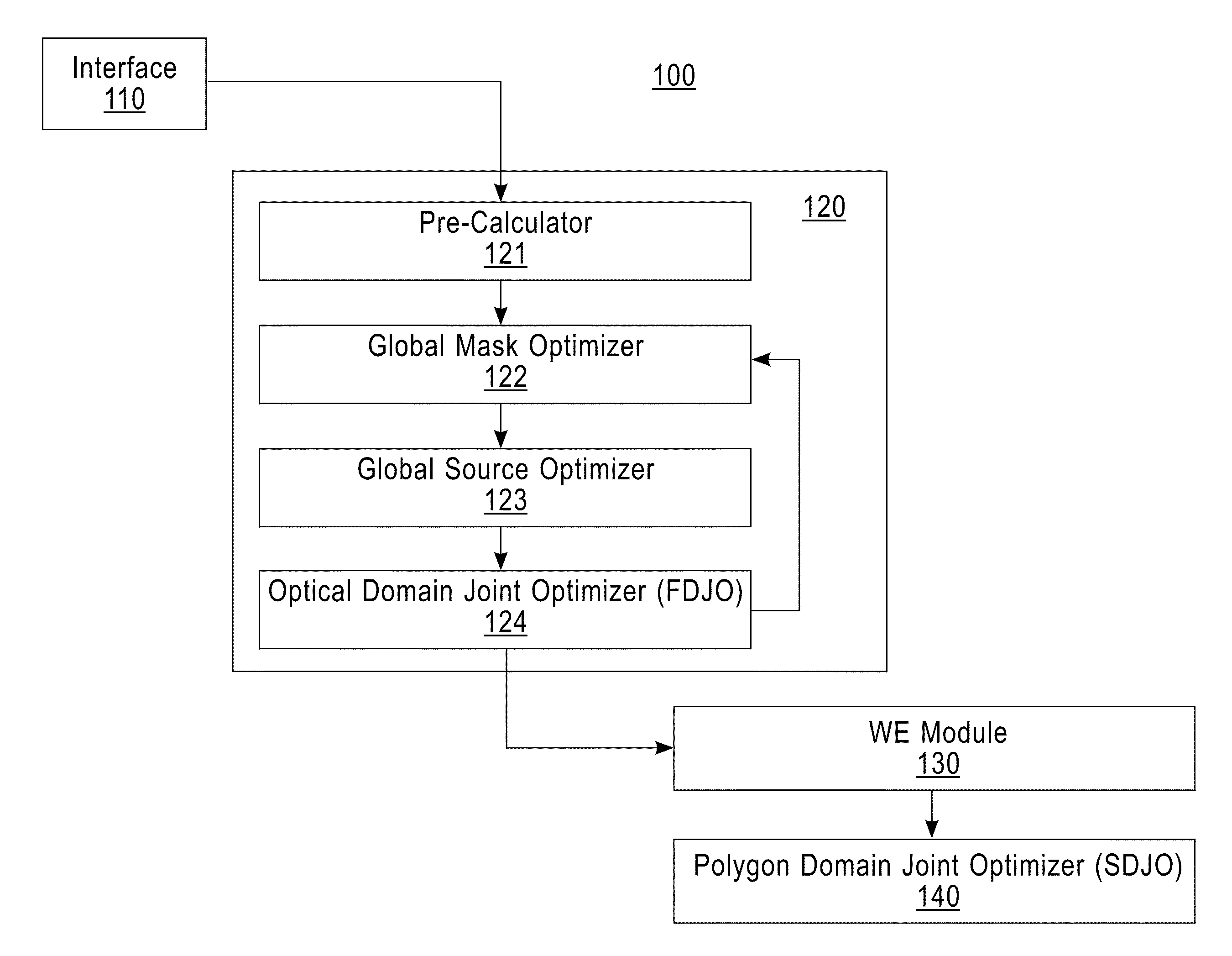
[0040]The present invention uses optical domain masks as variables during the SMO process optimization; however, the mask topology in the pupil domain is converted to the polygon domain expression at the later wavefront engineering step eventually in order to apply further improved mask optimization. In the optical domain, wavefronts are optimized according to SMO (Source Mask Optimization) technique, in a preferred embodiment.

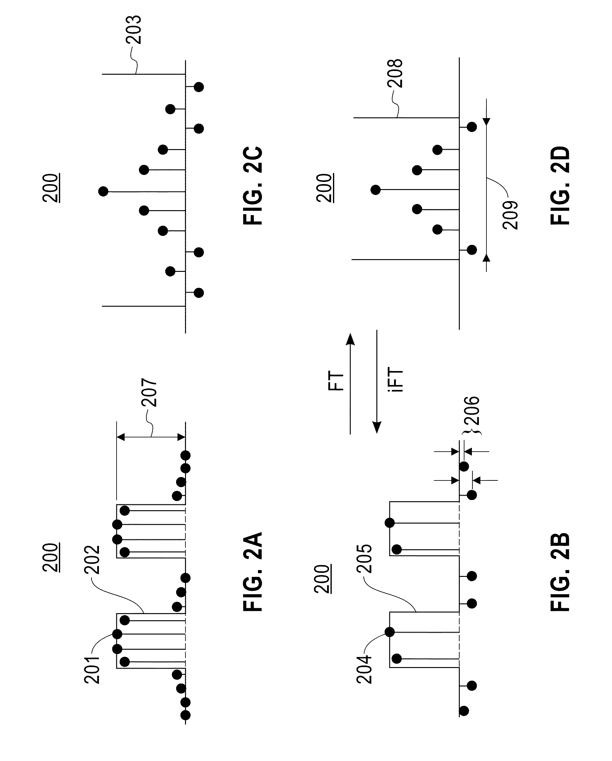
[0041]In general, the invention includes a step in which a set of optical domain variables is generated to represent the mask wavefront during optimization, and these variables can be located in the object domain or in the pupil domain. In some embodiments, the present invention uses object domain ...


PUM

PropertyMeasurementUnit
feature sizeaaaaaaaaaa
sizeaaaaaaaaaa
sizeaaaaaaaaaa

Abstract

A method, an article of manufacture, and a system for designing a mask. The method for designing a mask is implemented by a computer device having a memory, a processor device communicatively coupled to the memory, and a module configured to carry out the method including the steps of: generating an optical domain representation from a design pattern and an imaging light; and optimizing the optical domain representation under a constraint that values of negative excursions at predetermined evaluation points must be greater than or equal to predetermined negative threshold values assigned to the predetermined evaluation points; where: the optical domain representation is a variable representation of a wavefront; the imaging light is light that is transmitted through the mask; the negative excursions are in an object domain representation of the optical domain representation; and the predetermined evaluation points are in the object domain representation.

Description

CROSS-REFERENCE TO RELATED APPLICATION[0001]This application claims priority under 35 U.S.C. ยง119 from Japan Patent Application No. 2012-084657 filed Apr. 3, 2012, the entire contents of which are incorporated herein by reference.BACKGROUND OF THE INVENTION[0002]1. Field of the Invention[0003]The present invention relates to a mask design technology and more particularly relates to a mask design method, a program therefore, and a mask design system.[0004]2. Description of Related Art[0005]The entire contents of US Patent applications identified by Ser. Nos. 12 / 334,482, 12 / 334,488 each filed on Dec. 14, 2008; Ser. No. 12 / 334,485 filed on Dec. 14, 2008; and the entire contents of U.S. Pat. No. 8,108,802 issued on Jan. 31, 2012; and of U.S. Pat. No. 7,057,709 issued on Jun. 6, 2006; may be incorporated herein as references.[0006]Minimum printed feature sizes in semiconductor devices become finer due to continuous requirements for ever higher performance and faster operation of the devi...

Claims


Application Information

Patent Timeline
17 Feb 2015
Publication
US8959462B2
IPC
G06F17/50; G03F1/70
CPC
G03F1/70
Inventors
INOUE, TADANOBU; MELVILLE, DAVID O