Pixel information management apparatus and image capture apparatus using the same
a technology of information management apparatus and image capture apparatus, which is applied in the direction of instruments, television systems, static indicating devices, etc., to achieve the effect of efficient storage of information
- Summary
- Abstract
- Description
- Claims
- Application Information
AI Technical Summary
Benefits of technology
Problems solved by technology
Method used
Image
Examples
first embodiment
[0028
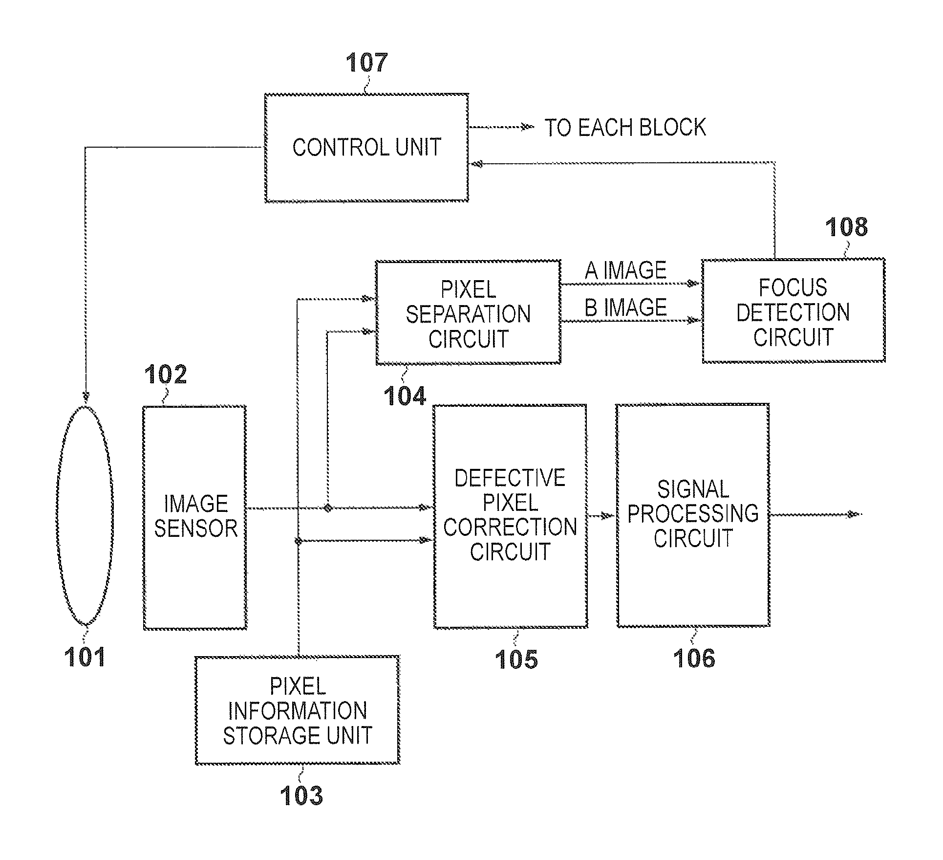
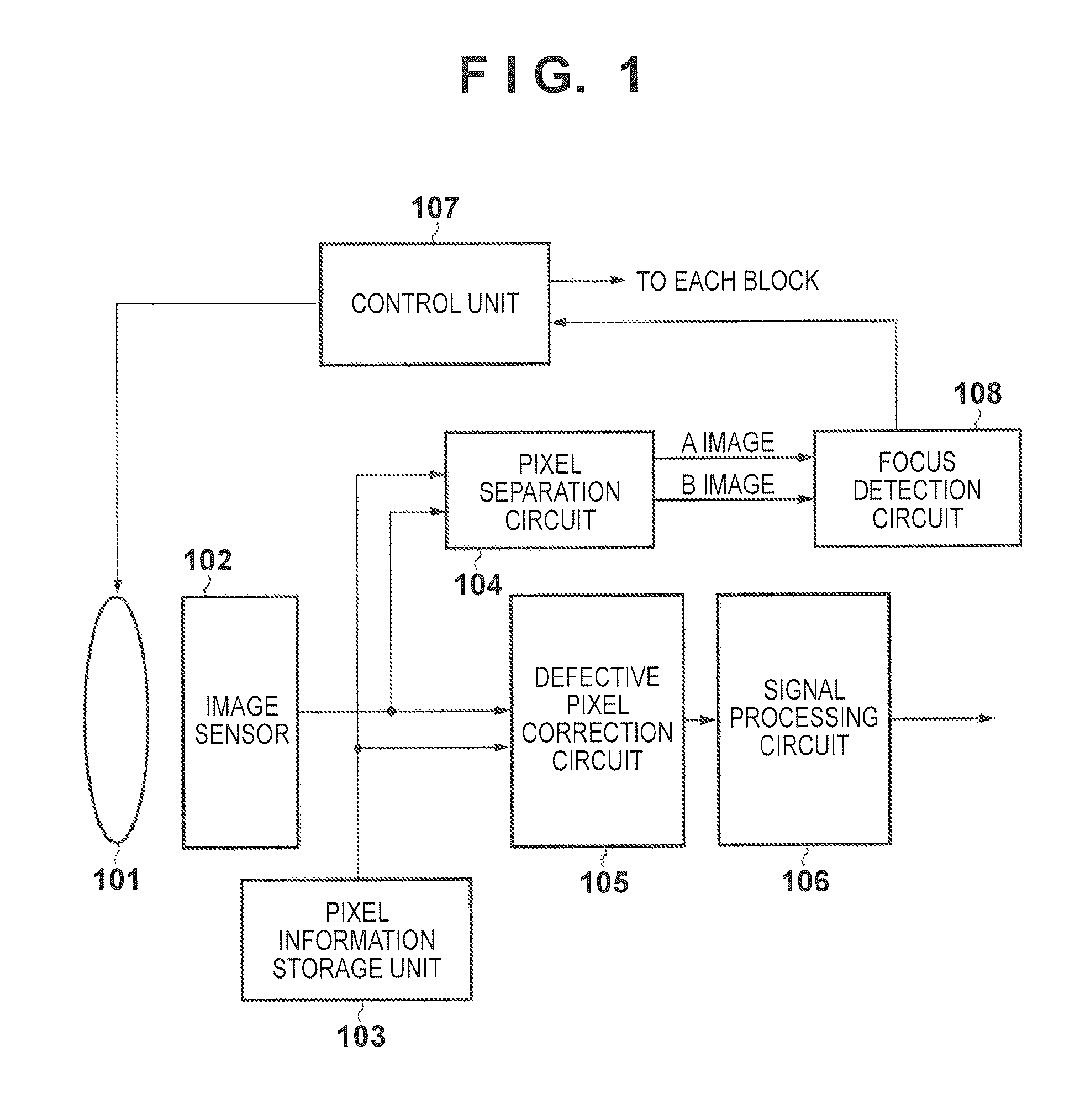
[0029]FIG. 1 is a block diagram showing an example of the functional configuration of a digital camera serving as one example of an apparatus to which a pixel information management apparatus according to a first embodiment of the present invention is applicable.
[0030]An image capture lens 101 has a focus lens that is driven in accordance with the control of a control unit 107, and forms an object image on the image capture plane of an image sensor 102. The image sensor 102 is a photoelectric conversion sensor such as a CCD image sensor or a CMOS image sensor, and a plurality of pixels are laid out thereon. The image sensor 102 has imaging pixels and focus detection pixels. A pixel information storage unit 103 that is one form of a pixel information management apparatus stores position information on defective pixels and focus detection pixels. Note that both imaging pixels and focus detection pixels may be defective pixels. A pixel separation circuit 104 generates a pair of im...
second embodiment
[0063
[0064]Next, a second embodiment of the present invention will be described, with reference to FIG. 7. Similarly to the first embodiment, the present embodiment is described using a digital camera to which a pixel information storage apparatus according to the present invention is applied as an example. In FIG. 7, the same reference numerals as in FIG. 1 are given to configurations similar to those in the first embodiment.
[0065]In the first embodiment, a configuration was adopted in which the defective pixel correction circuit 105 and the pixel separation circuit 104 are connected in parallel to the pixel information storage unit 103. In contrast, in the present embodiment, the pixel separation circuit 104 and the defective pixel correction circuit 105 are wired in series, and a second pixel information storage unit 109 is added, in addition to the first pixel information storage unit 103 in which pixel information similar to that in the pixel information storage unit in the fir...
third embodiment
[0071
[0072]Next, a third embodiment of the present invention will be described, with reference to FIG. 8. Similarly to the first embodiment, the present embodiment is described using a digital camera to which a pixel information storage apparatus according to the present invention is applied as an example. In FIG. 8, the same reference numerals as in FIG. 1 are given to configurations similar to those in the first embodiment.
[0073]In the present embodiment, a third pixel information storage unit 110 is added in addition to the first pixel information storage unit 103 corresponding to the pixel information storage unit. Also, a switch 111 is provided so as to selectively connect either the first pixel information storage unit 103 or the third pixel information storage unit 110 with the pixel separation circuit 104 and the defective pixel correction circuit 105 according to control of the control unit 107.
[0074]There is a case where the image sensor 102 has a plurality of reading mode...
PUM
 Abstract
Description
Claims
Application Information


