
Touch screen panel and fabrication method thereof

a technology of touch screen and fabrication method, applied in the field of touch screen panel, can solve the problems of reducing the overlap area of the intersecting region, deteriorating the sensitivity sensed by each sensing pattern, and large capacity for parasitic capacitance accordingly, so as to reduce or eliminate the vulnerability to static electricity

Active Publication Date: 2015-04-07
SAMSUNG DISPLAY CO LTD
View PDF31 Cites 2 Cited by
  • Summary
  • Abstract
  • Description
  • Claims
  • Application Information

AI Technical Summary

Benefits of technology

The patent aims to reduce the risk of static electricity damage in touch screen panels by using a low resistance metal material for connection patterns between sensing cells. This helps to prevent electrostatic discharge (ESD) issues.

Problems solved by technology

However, an overlapping area of each connection part disposed on the upper and lower layers becomes large and the capacity for parasitic capacitance accordingly becomes large, such that the sensitivity sensed by each sensing pattern deteriorates.
However, even in this case, the connection part connecting the first sensing patterns is still made of the transparent conductive material having a high resistance value and reduces the overlapping area of the intersecting region.
Also, since the connection pattern is disposed on the upper portion of the insulating layer, it is vulnerable to static electricity applied or occurring from the outside.

Method used


Image

  • Touch screen panel and fabrication method thereof
  • Touch screen panel and fabrication method thereof
  • Touch screen panel and fabrication method thereof

Examples


Embodiment Construction

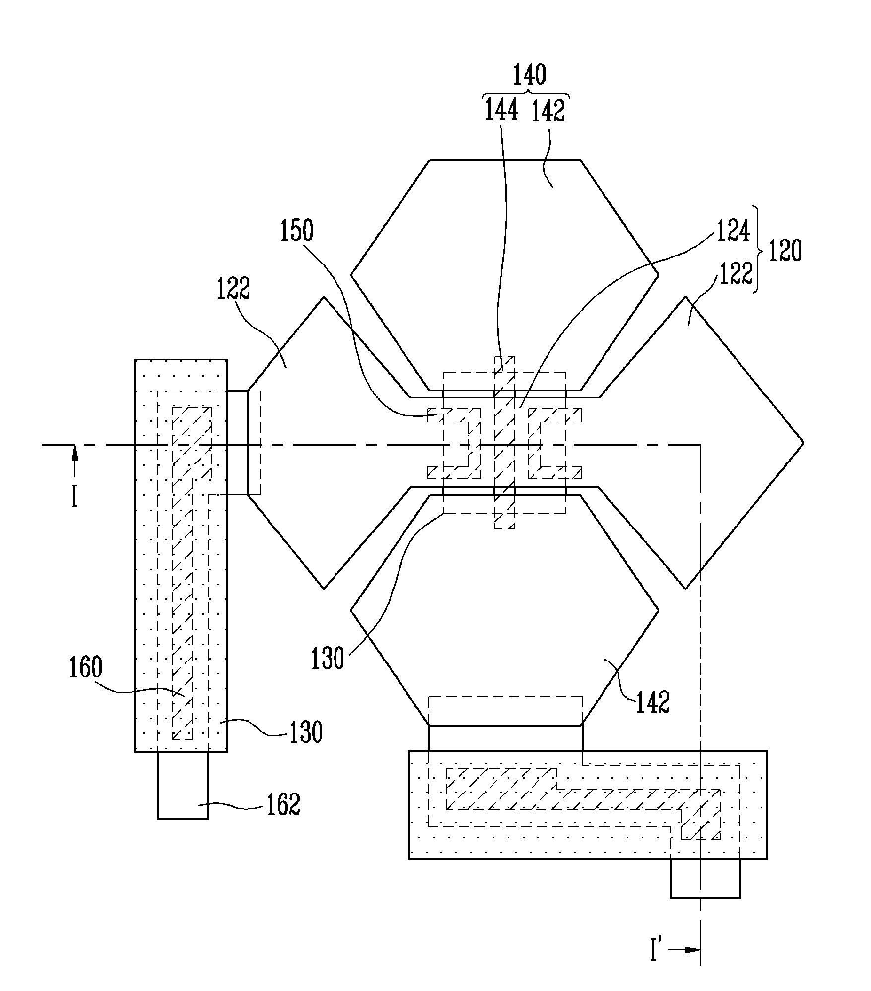
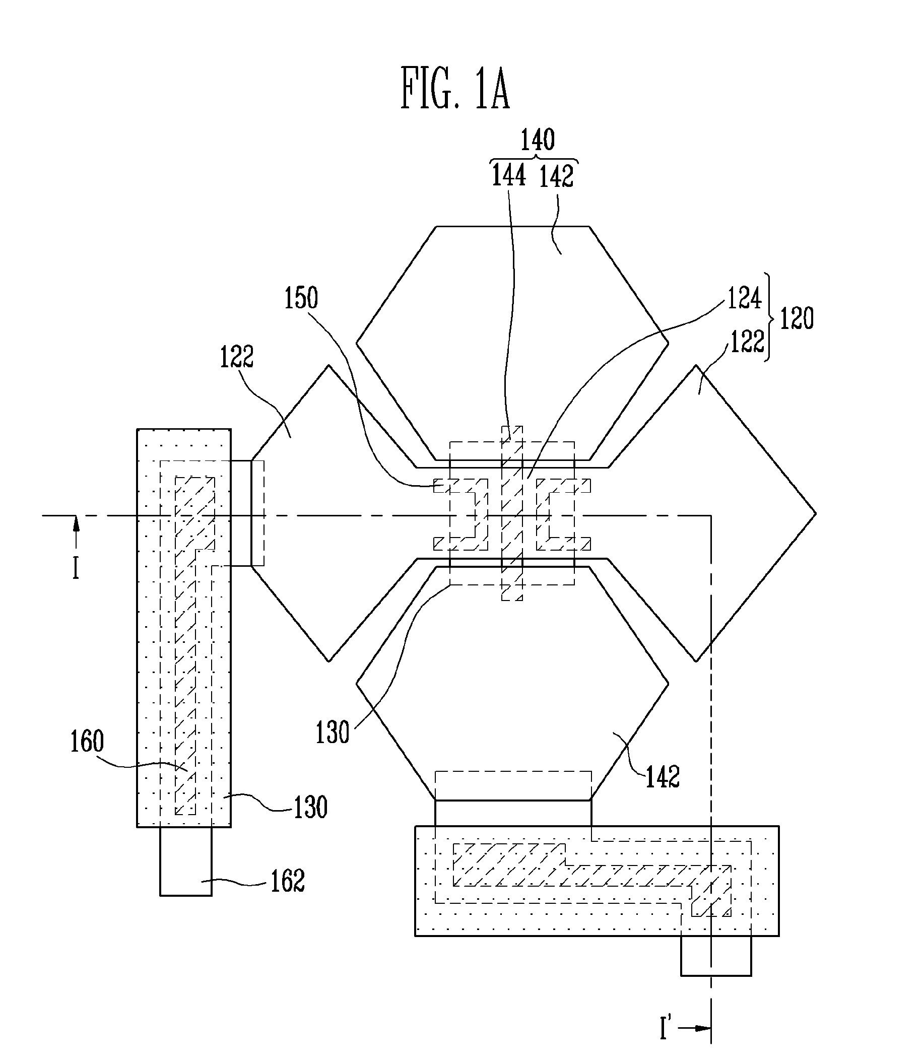
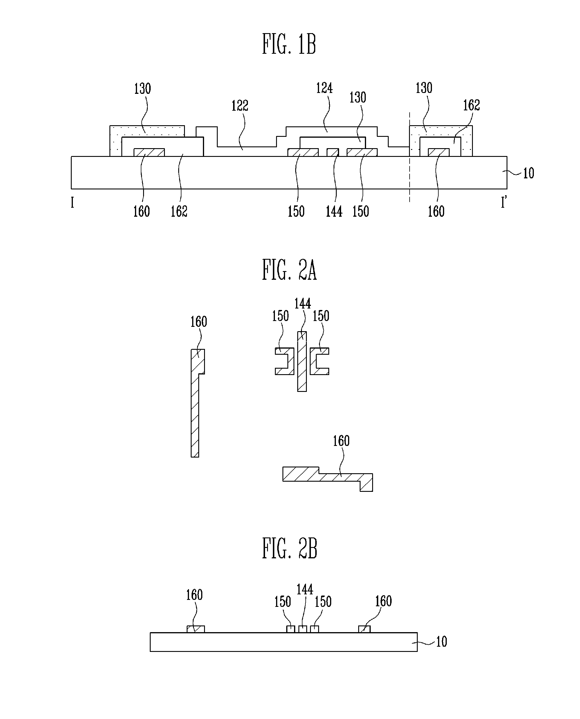
[0031]In the following detailed description, only certain exemplary embodiments of the present invention have been shown and described, simply by way of illustration. As those skilled in the art would realize, the described embodiments may be modified in various different ways, all without departing from the spirit or scope of the present invention. Accordingly, the drawings and description are to be regarded as illustrative in nature and not restrictive. In addition, when an element is referred to as being “on,”“disposed on” or “formed on” another element, it can be directly on the another element or be indirectly on the other element with one or more intervening elements interposed therebetween. Also, when an element is referred to as being “connected to” another element, it can be directly connected to the other element or be indirectly connected to the other element with one or more intervening elements interposed therebetween. Furthermore, the structures on the same level can b...


PUM


Abstract

A touch screen panel including: a transparent substrate that incorporate a display region and a non-display region; first sensing patterns that are arranged in a first direction and include first sensing cells and first connection parts; second sensing patterns that are arranged in a second direction and include second sensing cells and second connection parts; an insulating layer that is formed on each of the second connection parts in an island shape; the second sensing cells contact the ends of exposed second connection parts; a plurality of first sensing cells that are arranged on the display region in the first direction intersecting with the second direction; connection parts that connect the adjacent first sensing cells to each other; and metal patterns that are formed in the non-display region and are connected to each of the sensing cells disposed at the ends of the display region.

Description

CROSS-REFERENCE TO RELATED APPLICATION[0001]This application claims the benefit of Korean Patent Application No. 10-2010-0023239, filed on Mar. 16, 2010 in the Korean Intellectual Property Office, the disclosure of which is incorporated herein by reference.BACKGROUND[0002]1. Field of the Invention[0003]Aspects of the present invention relate to a touch screen panel and a fabrication method thereof, and more particularly, to a touch screen panel integrally formed on an upper substrate of a flat panel display and a fabrication method thereof.[0004]2. Description of the Related Art[0005]A touch screen panel is an input device that selects contents displayed on a screen such as an image display device, etc. using a person's hand or an object to input commands of a user.[0006]To this end, a touch screen panel is provided on the front face of the image display device and converts positions directly contacting a person's hand or an object into electrical signals. Therefore, the command con...

Claims


Application Information

Patent Timeline
Patent Type & Authority Patents(United States)
IPC IPC(8): G06F3/041G06F3/044
CPCG06F3/044G06F2203/04111G06F3/0443G06F3/0446G06F2203/04103
Inventor RHO, SOO-GUYCHO, SE-ILLEE, JAE-HYUNYI, CHUNG
Owner SAMSUNG DISPLAY CO LTD
Learn More