Imaging systems for optical computing devices

a technology of optical computing and optical train, applied in the field of optical computing systems, can solve the problems of difficult field analysis conditions, expensive and complex transition of spectroscopic instruments from laboratories into field or process environments, and delay in obtaining analysis,

Active Publication Date: 2015-04-21
HALLIBURTON ENERGY SERVICES INC
View PDF141 Cites 26 Cited by
  • Summary
  • Abstract
  • Description
  • Claims
  • Application Information

AI Technical Summary

Problems solved by technology

Thus, there is usually a delay in obtaining an analysis due to sample preparation time, even discounting the transit time of transporting the sample to a laboratory.
Furthermore, the transitioning of spectroscopic instruments from a laboratory into a field or process environment can be expensive and complex.
Furthermore, sample preparation, when required, can be difficult under field analysis conditions.
The difficulty of performing sample preparation in the field can be especially problematic in the presence of interfering materials, which can further complicate conventional spectroscopic analyses.
Quantitative spectroscopic measurements can be particularly challenging in both field and laboratory settings due to the need for precision and accuracy in sample preparation and spectral interpretation.

Method used


Image

  • Imaging systems for optical computing devices
  • Imaging systems for optical computing devices
  • Imaging systems for optical computing devices

Examples


Embodiment Construction

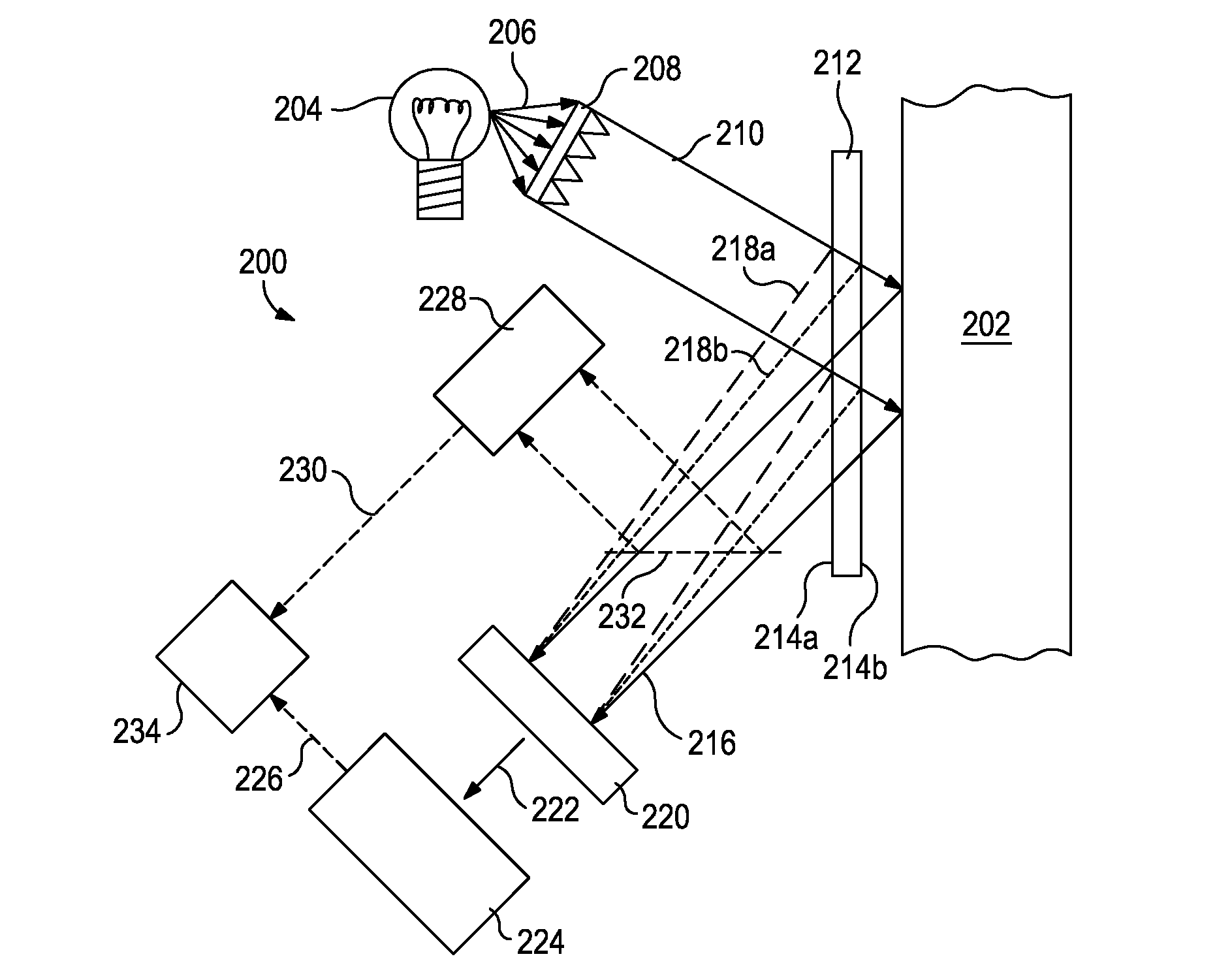
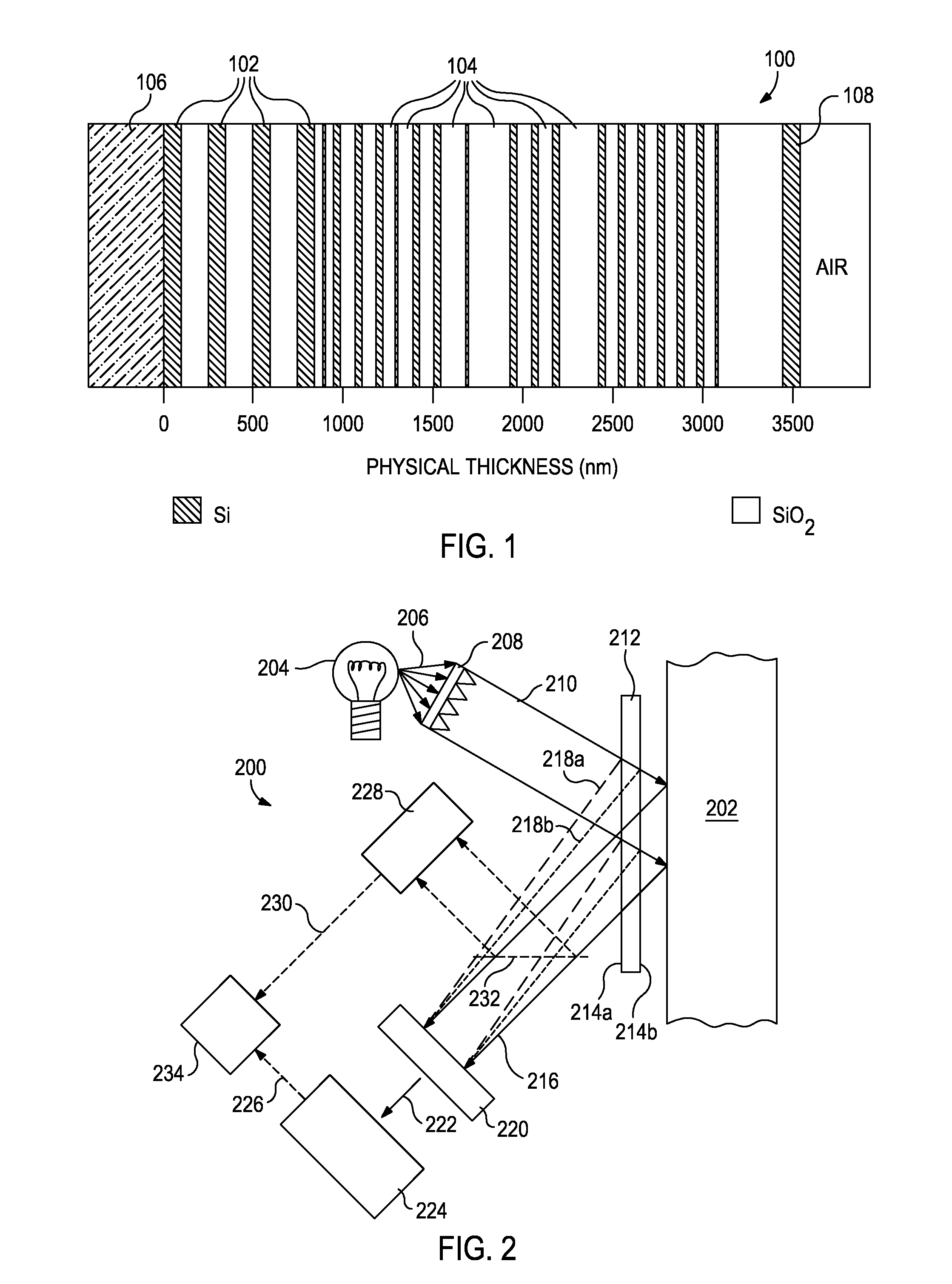
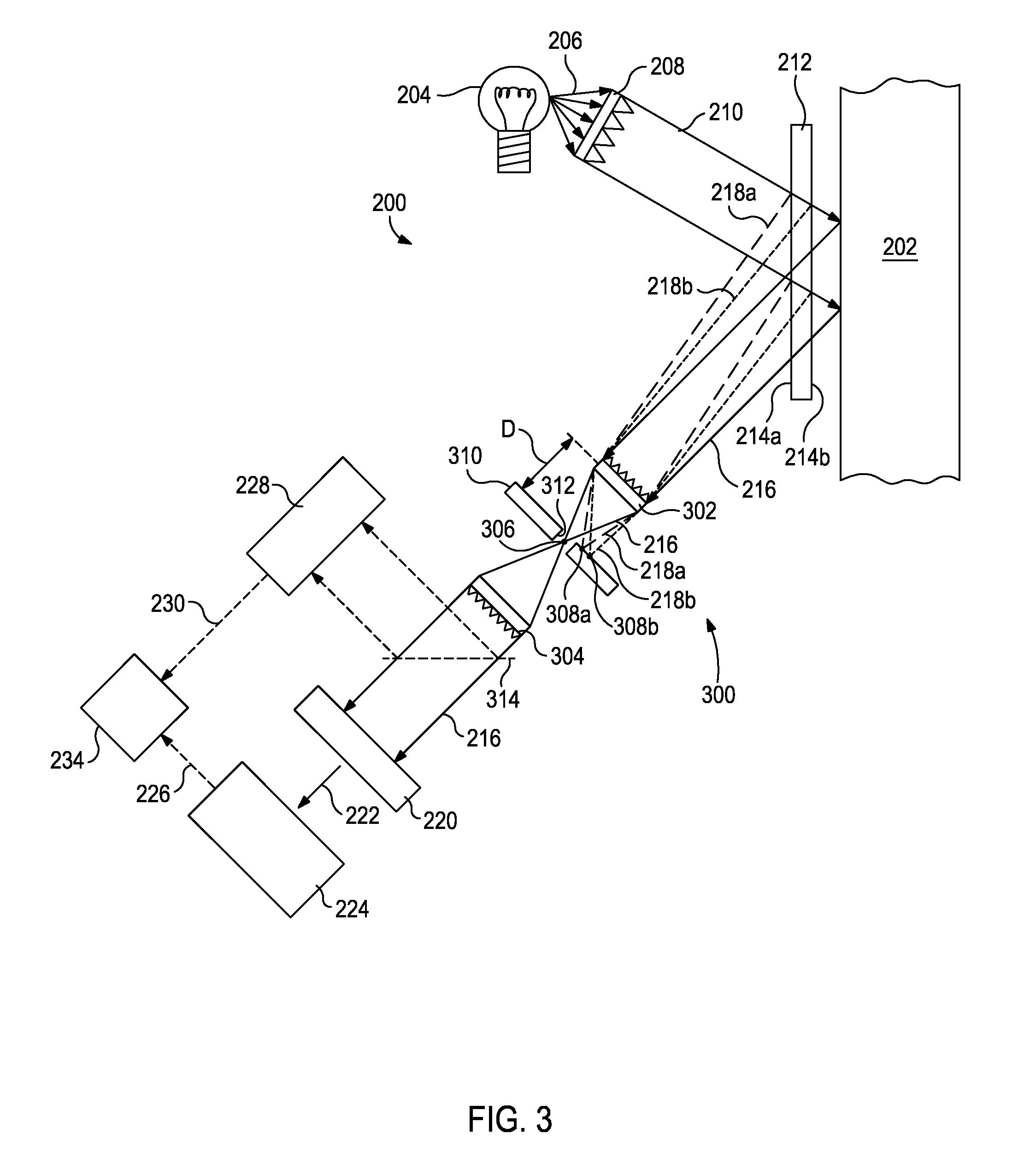
[0017]The present invention generally relates to systems and methods of optical computing and, more specifically, to imaging systems for an optical train in an optoanalytical device.

[0018]Embodiments described herein include various configurations of imaging systems that can be used in optical computing devices, also commonly referred to as opticoanalytical devices, in order to improve sensitivity and detection limits of the optical computing devices. The exemplary imaging systems may be suitable for use in optical computing devices as employed in the oil and gas industry. For example, optical computing devices provide a relatively low cost, rugged, and accurate system for monitoring petroleum quality for the purpose of optimizing decision making at a well site and efficient management of hydrocarbon production. In some applications, the imaging systems disclosed herein may be useful in improving detection limits when determining a particular characteristic of a substance, compound,...


PUM

PropertyMeasurementUnit
transmissionaaaaaaaaaa
electromagnetic radiationaaaaaaaaaa
anglesaaaaaaaaaa

Abstract

Optical computing devices are disclosed. One optical computing device includes an electromagnetic radiation source that emits electromagnetic radiation into an optical train to optically interact with a sample and at least one integrated computational element, the sample being configured to generate optically interacted radiation. A sampling window is arranged adjacent the sample and configured to allow transmission of the electromagnetic radiation therethrough and has one or more surfaces that generate one or more stray signals. A first focal lens is arranged to receive the optically interacted radiation and the one or more stray signals and generate a primary focal point from the optically interacted radiation. A structural element defines a spatial aperture aligned with the primary focal point such that the optically interacted radiation is able to pass therethrough while transmission of the one or more stray signals is substantially blocked by the structural element.

Description

BACKGROUND[0001]The present invention generally relates to systems and methods of optical computing and, more specifically, to imaging systems for an optical train in an optoanalytical device.[0002]Spectroscopic techniques for measuring various characteristics of materials are well known and are routinely used under laboratory conditions. In some cases, these spectroscopic techniques can be carried out without using an involved sample preparation. It is more common, however, to carry out various sample preparation steps before conducting the analysis. Reasons for conducting sample preparation steps can include, for example, removing interfering background materials from the analyte of interest, converting the analyte of interest into a chemical form that can be better detected by the chosen spectroscopic technique, and adding standards to improve the accuracy of quantitative measurements. Thus, there is usually a delay in obtaining an analysis due to sample preparation time, even di...

Claims


Application Information

Patent Timeline
Patent Type & Authority Patents(United States)
IPC IPC(8): G01N21/00G01N21/31G01N21/59G01N21/85G06E3/00
CPCG01N21/59G06E3/00G01N21/31G01N21/85G06E3/001G01N2201/064
Inventor FREESE, ROBERTJONES, CHRISTOPHER MICHAELPERKINS, DAVIDSIMCOCK, MICHAELSOLTMANN, WILLIAM
Owner HALLIBURTON ENERGY SERVICES INC
Why Eureka
Try Eureka