Advanced device assembly structures and methods

a technology of advanced devices and assembly structures, applied in the field of advanced device assembly structures and methods, can solve the problems of lateral deformation, increased widening, and lack of joint masses,

Active Publication Date: 2015-05-05
INVENSAS LLC
View PDF19 Cites 20 Cited by
  • Summary
  • Abstract
  • Description
  • Claims
  • Application Information

AI Technical Summary

Problems solved by technology

The use of such joining masses can have some deficiencies, however, in particular such joints, when melted in order to form joints between, for example, contact pads or the like, can undergo lateral deformation.
Further, such widening can increase during normal use of the microelectronic assembly due to heating of the joints.
This dishing can adversely affect bond strength and is generally not desirable.

Method used


Image

  • Advanced device assembly structures and methods
  • Advanced device assembly structures and methods
  • Advanced device assembly structures and methods

Examples


Embodiment Construction

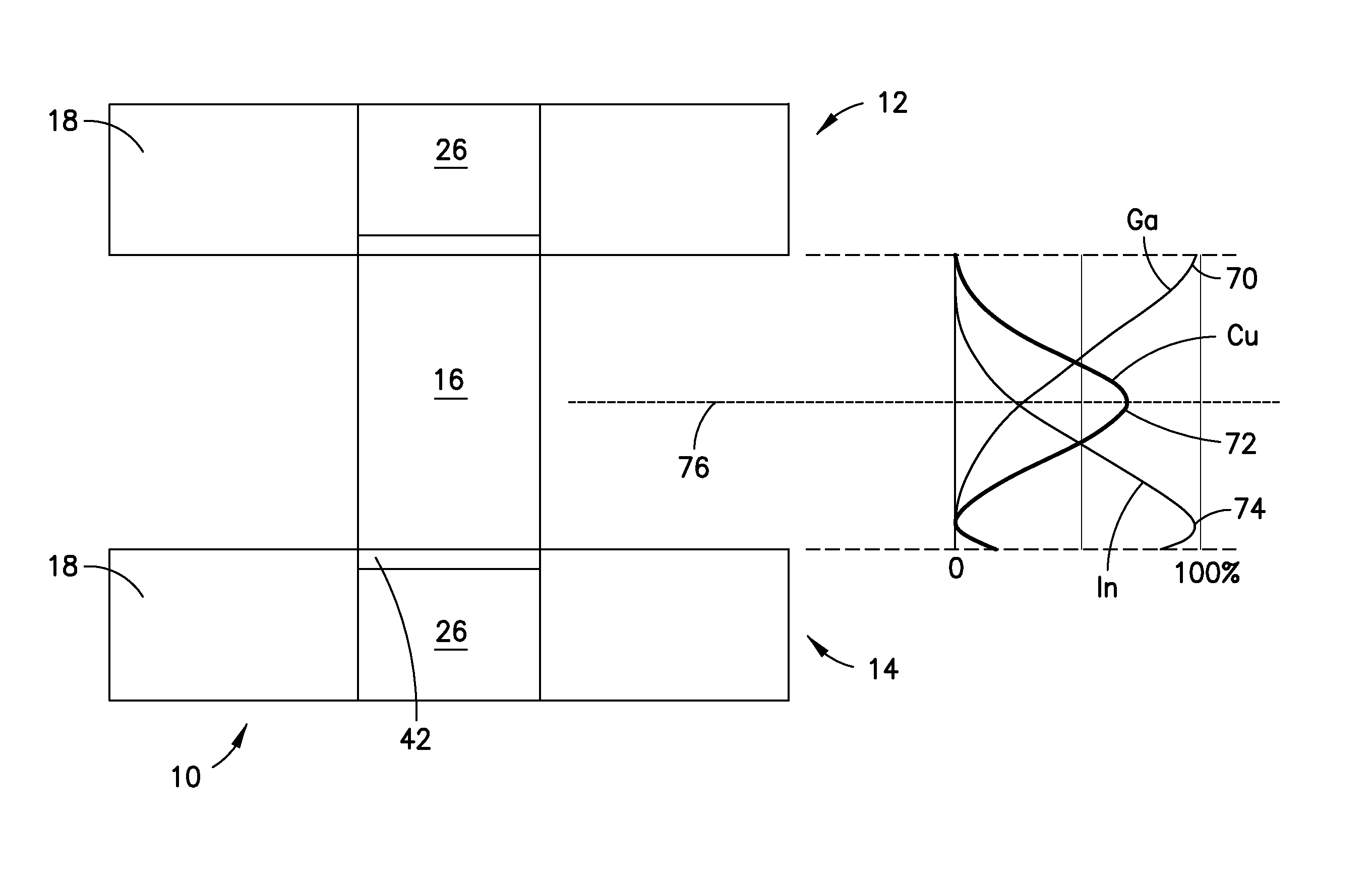
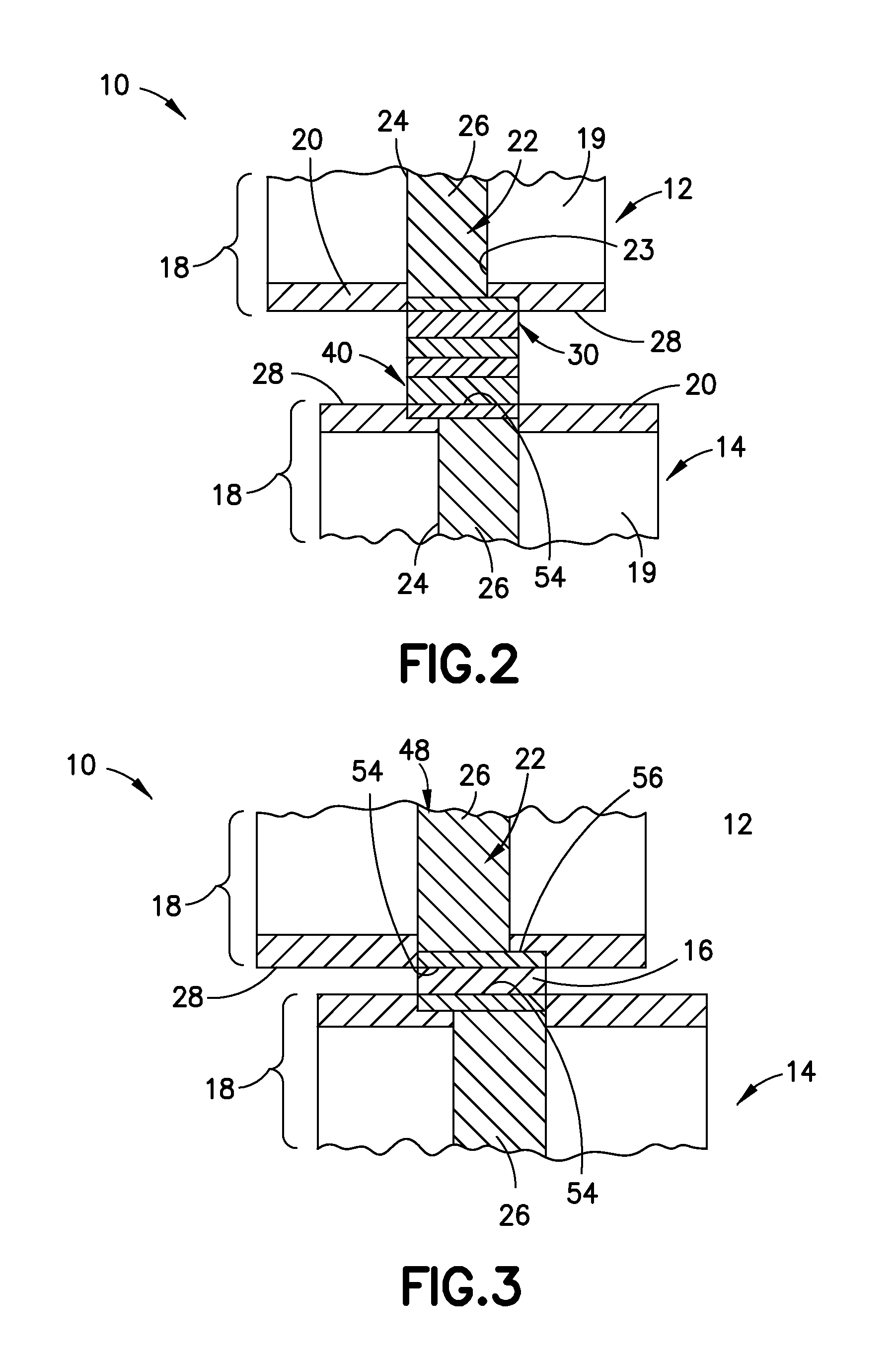
[0041]Turning to the Figures, wherein similar numeric references are used in connection with similar features, FIG. 3 shows a microelectronic assembly 10 according to an aspect of the present disclosure. Assembly 10 includes first and second elements joined together by an alloy mass 16. In FIG. 3, which shows alloy mass 16 joining the elements of FIG. 2, the first and second elements are shown as portions of microelectronic devices, which can be in the form of packaged microelectronic elements, interposers, substrates, or the like. For example, first and second elements 12 and 14 are shown in FIGS. 2-33 as including a support material layer 18 that can, for example be of a semiconductor or a dielectric material layer such as found in an interposer structure, in a portion of a packaged microelectronic element, or in a portion of a semiconductor die. In an example, support material layer 18 can of one of a semiconductor material, or of a dielectric material, or of a combination of sem...


PUM

PropertyMeasurementUnit
thicknessaaaaaaaaaa
melting pointaaaaaaaaaa
melting pointsaaaaaaaaaa

Abstract

A microelectronic assembly includes a first substrate having a surface and a first conductive element and a second substrate having a surface and a second conductive element. The assembly further includes an electrically conductive alloy mass joined to the first and second conductive elements. First and second materials of the alloy mass each have a melting point lower than a melting point of the alloy. A concentration of the first material varies in concentration from a relatively higher amount at a location disposed toward the first conductive element to a relatively lower amount toward the second conductive element, and a concentration of the second material varies in concentration from a relatively higher amount at a location disposed toward the second conductive element to a relatively lower amount toward the first conductive element.

Description

BACKGROUND OF THE INVENTION[0001]Packaged microelectronic devices and related connection components, such as interposers or the like, use various structures to facilitate attachment with other packaged microelectronic devices or connection components to form various microelectronic assemblies. Such structures can include contact pads in the form of enlarged areas of a conductive metal exposed at surfaces of the devices or components. Alternatively, such structures can be in the form of exposed ends of metalized vias, conductive pins, posts, or the like. When aligned with similar connection features in another device or component, the connection features can be joined together using, for example, a conductive joining material, such as a solder mass or the like. Solder masses, such as solder mass 1 shown in FIG. 1A are often used to form such joints because they can be easy to join between structures due to their relatively low melting temperature. Further, such conductive joining mas...

Claims


Application Information

Patent Timeline
Patent Type & Authority Patents(United States)
IPC IPC(8): H05K1/16H01L21/48H01L21/50H01L21/768H01L23/00H01L23/10H01L23/48H01L23/498H05K13/04
CPCH05K13/046H01L23/10H01L21/50H01L24/13H01L24/14H01L24/16H01L24/73H01L24/81H01L24/98H01L23/49811H01L2224/05027H01L2224/13155H01L2224/13184H01L2224/1319H01L2224/16146H01L2224/16235H01L2224/16505H01L2224/2745H01L2224/05569H01L2224/1308H01L2224/13076H01L2224/14131H01L2224/32505H01L2224/27462H01L2224/27464H01L2224/81825H01L2224/16501H01L21/76898H01L23/481H01L24/02H01L24/03H01L24/05H01L24/11H01L24/27H01L2224/02372H01L2224/0401H01L2224/05025H01L2224/05026H01L2224/05138H01L2224/05155H01L2224/05157H01L2224/05164H01L2224/05166H01L2224/05171H01L2224/0518H01L2224/05181H01L2224/05184H01L2224/05187H01L2224/05571H01L2224/05647H01L2224/1145H01L2224/11452H01L2224/11462H01L2224/11464H01L2224/1147H01L2224/13009H01L2224/13017H01L2224/13022H01L2224/13023H01L2224/13025H01L2224/13078H01L2224/13082H01L2224/13105H01L2224/13109H01L2224/13147H01L2224/27452H01L2224/29011H01L2224/29023H01L2224/2908H01L2224/29082H01L2224/29109H01L2224/29147H01L2224/32225H01L2224/32245H01L2224/32501H01L2224/73103H01L2224/73203H01L2224/81075H01L2224/8112H01L2224/81193H01L2224/83075H01L2224/8312H01L2224/83193H01L2224/83825H01L2924/381H01L2224/05568H01L2224/03912H01L2224/05023H01L2224/81141H01L2224/29138H01L2224/29105H01L2224/13138H01L21/4853H01L2924/00014H01L2924/04953H01L2924/01071H01L2924/01042H01L2924/01015H01L2924/04941H01L2924/01074H01L2924/01047H01L2924/01031H01L2924/01034H01L2924/00012H01L2924/07025H01L2224/13018H01L24/29H01L24/32H01L24/83H01L2224/05552H05K1/111H05K1/144H05K1/14H05K1/18H05K2201/04H05K1/11H01L2224/16503H01L2224/16145H01L2224/13083H01L23/49B23K20/002B23K20/023H05K3/0094H05K3/34H05K13/0465H05K2203/04
Inventor UZOH, CYPRIAN EMEKA
Owner INVENSAS LLC
Why Eureka
Try Eureka