Method for treating SiOCH film with hydrogen plasma

a technology of hydrogen plasma and sioch film, which is applied in the direction of basic electric elements, semiconductor/solid-state device manufacturing, electric apparatus, etc., can solve the problems of signal delay and increase in power consumption associated with multi-layer wiring structure, reduced advantage of using copper, and complicated process to prevent copper from diffusing in the sioch film

Active Publication Date: 2015-05-12
ASM IP HLDG BV
View PDF2 Cites 386 Cited by
  • Summary
  • Abstract
  • Description
  • Claims
  • Application Information

AI Technical Summary

Benefits of technology

[0010]Some embodiments provide technology to form a gap-fill dielectric film constituted by a SiOCH film exhibiting low film-shrinkage during high-temperature UV-curing and therefore to inhibit disconnection of wiring lines and cracks of the dielectric film, which SiOCH film is deposited by flowable CVD, ALD, spin coating, or the like.

Problems solved by technology

As the miniaturization of interconnection progresses, signal delay and increase in power consumption associated with increase of wiring capacitance especially in a multilayer wiring structure have become a problem.
However, as the miniaturization of interconnection has further progressed, the resistance of copper as the wiring material rises according to the width of the interconnection, and therefore the advantage of using copper has diminished.
By its nature, copper easily defuses in the SiOCH film, and therefore when copper is used as the wiring material, a complicated process to prevent copper from diffusing in the SiOCH film is required.
In this case, since extremely narrow intervals are formed between metal wiring lines, the intervals are not filled completely by the conventional CVD method, and accordingly voids and the like are formed in the interlayer dielectric film.
However, after tungsten wiring is complete, followed by filling intervals between the wiring lines with a SiOCH film by flowable CVD, ALD, or spin coating, when UV-curing is conducted for lowering dielectric constant and stabilization of the film, film shrinkage occurs.
If film shrinkage is significant, disconnection of wiring lines and collapse of wiring lines occur due to shrinking force.
Further, cracks of the film itself may occur.
However, once the film is heated, film shrinkage during high-temperature UV-curing remains high and is not significantly improved.

Method used


Image

  • Method for treating SiOCH film with hydrogen plasma
  • Method for treating SiOCH film with hydrogen plasma
  • Method for treating SiOCH film with hydrogen plasma

Examples


example 1

H2 Plasma Treatment+High-Temperature UV-Curing

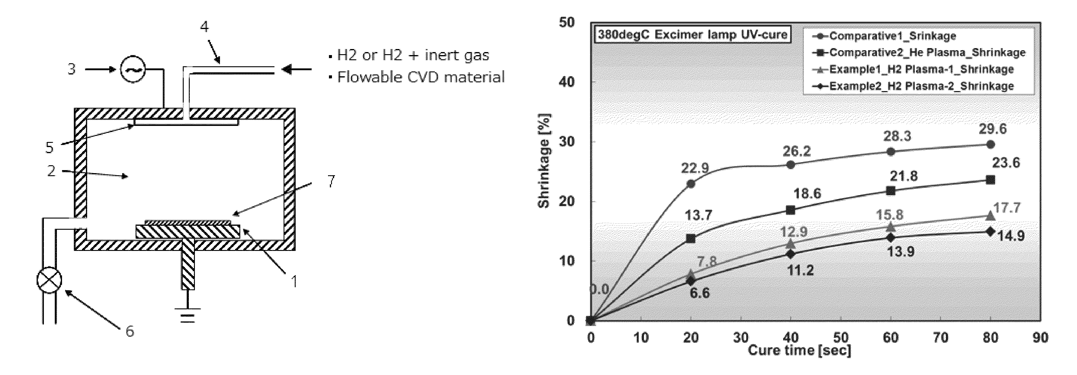
[0056]H2 plasma treatment was conducted on the film-deposited substrate in the same reaction chamber under conditions shown in Table 7 below.

[0057]

TABLE 7Substrate TemperatureRoom temperatureProcess Pressure500PaGas flow of H20.35 SLMRF power400 WDistance between electrodes8 mmDuration of H2 plasma treatment5 minutes

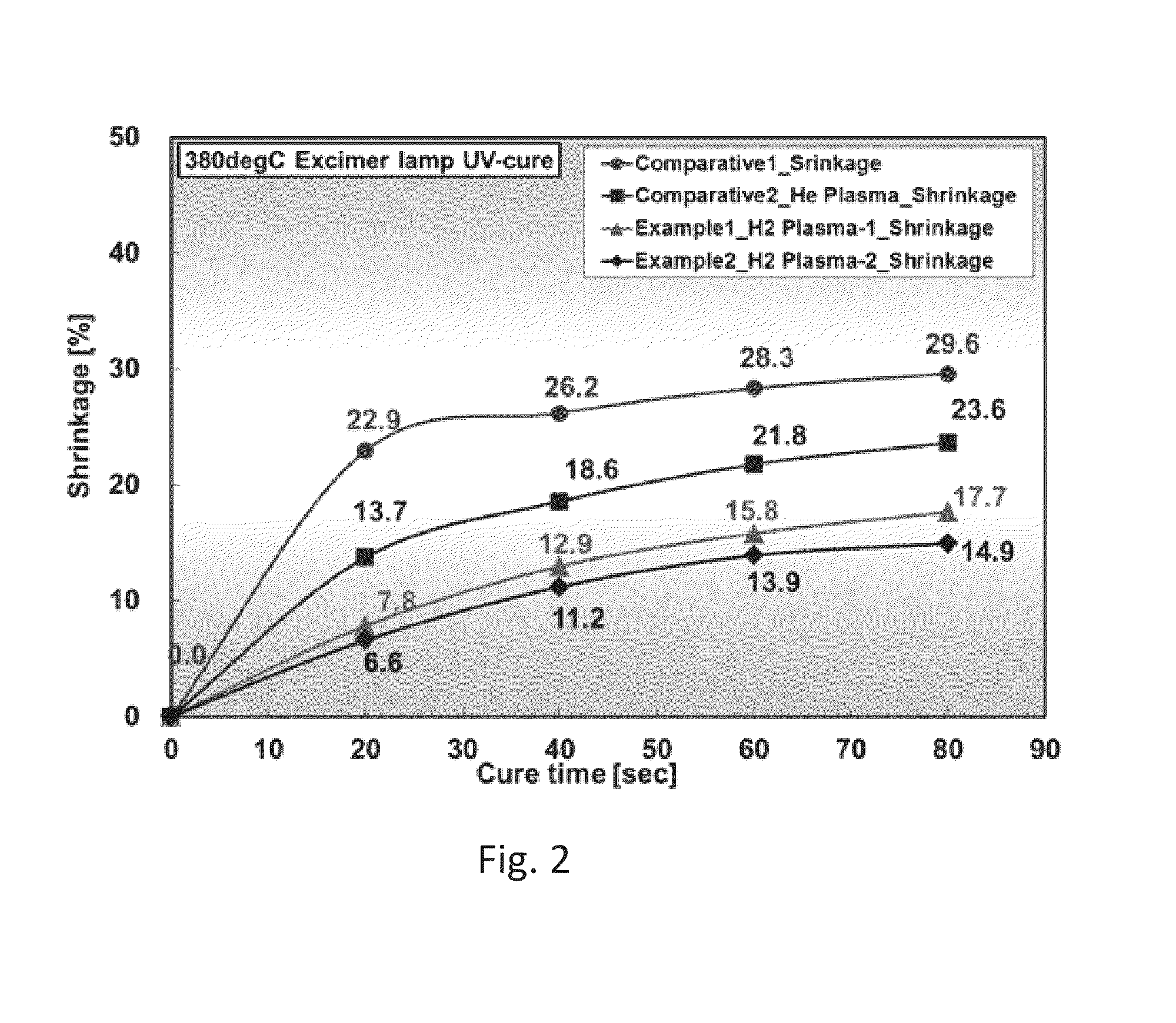
[0058]After the H2 plasma treatment, UV-curing was conducted in the same manner as in Comparative Example 2. Thereafter, film shrinkage was measured. The result is shown in FIG. 2 which is a graph showing the relationship between shrinkage [%] and cure time [sec]. As shown in FIG. 2, the film shrinkage by the UV-curing for 80 seconds was 17.7% which was about 25% lower than the film shrinkage when conducting He plasma treatment in Comparative Example 2. The mechanical strength of the film was also measured, and it was 9.2 GPa.

example 2

H2 Plasma Treatment+High-Temperature UV-Curing

[0059]H2 plasma treatment was conducted on the film-deposited substrate in the same reaction chamber under conditions shown in Table 8 below.

[0060]

TABLE 8Substrate TemperatureRoom temperatureProcess Pressure1100 PaGas flow of H20.5 SLMRF power400 WDistance between electrodes8 mmDuration of H2 plasma treatment5 minutes

[0061]After the H2 plasma treatment, UV-curing was conducted in the same manner as in Comparative Example 2. Thereafter, film shrinkage was measured. The result is shown in FIG. 2 which is a graph showing the relationship between shrinkage [%] and cure time [sec]. As shown in FIG. 2, the film shrinkage by the UV-curing for 80 seconds was 14.9% which was about 37% lower than the film shrinkage when conducting He plasma treatment in Comparative Example 2. The mechanical strength of the film was also measured, and it was 9.3 GPa.

[0062]Also, leakage current of the treated film was measured. The results are shown in FIG. 4. FIG. ...

example 3

Aminosilane Annealing+H2 Plasma Treatment+High-Temperature UV-Curing

[0063]Aminosilane annealing was conducted on the film-deposited substrate in the same reaction chamber under conditions shown in Table 9 below.

[0064]

TABLE 9Substrate TemperatureRoom temperatureAminosilaneDi-sec-buthylaminosilane (DSBAS)Process pressure15 PaDistance between electrodes 8 mmDuration of He plasma treatment60 seconds

[0065]After the aminosilane annealing, H2 plasma treatment was conducted on the film-deposited substrate in the same reaction chamber under conditions shown in Table 10 below.

[0066]

TABLE 10Substrate TemperatureRoom temperatureProcess Pressure1100 PaGas flow of H20.5 SLMRF power400 WDistance between electrodes8 mmDuration of H2 plasma treatment5 minutes

[0067]After the H2 plasma treatment, UV-curing was conducted in the same manner as in Comparative Example 3. Thereafter, film shrinkage was measured. The result is shown in FIG. 3 which is a graph showing the relationship between shrinkage [%] a...


PUM


Abstract

A method for forming a gap-fill SiOCH film on a patterned substrate includes: (i) providing a substrate having recessed features on its surface; (ii) filling the recessed features of the substrate with a SiOCH film which is flowable and non-porous; (iii) after completion of step (ii), exposing the SiOCH film to a plasma including a hydrogen plasma; and (iv) curing the plasma-exposed SiOCH film with UV light.

Description

BACKGROUND OF THE INVENTION[0001]1. Field of the Invention[0002]The present invention generally relates to technology of forming interlayer dielectric films for multilayer interconnection for semiconductor integrated circuits, particularly to a method for forming a gap-fill carbon-doped silicon oxide (SiOCH) film on a patterned surface of a substrate where recessed features between wiring lines are narrow.[0003]2. Description of the Related Art[0004]In recent years, the development of semiconductor devices has been remarkable, and has achieved high integration, high speed, and high capacity, and accordingly, the miniaturization of interconnection of semiconductor circuits has progressed. As the miniaturization of interconnection progresses, signal delay and increase in power consumption associated with increase of wiring capacitance especially in a multilayer wiring structure have become a problem. To solve the problem, an insulation film with a low dielectric constant, which is a S...

Claims


Application Information

Patent Timeline
Patent Type & Authority Patents(United States)
IPC IPC(8): H01L21/02
CPCH01L21/02126H01L21/02271H01L21/0228H01L21/02282H01L21/0234H01L21/02274H01L21/02277H01L21/02348
Inventor NAKANO, AKINORIUEDA, SHINTAROISHIKAWA, DAIMATSUSHITA, KIYOHIRO
Owner ASM IP HLDG BV
Why Eureka
Try Eureka