Touch sensor panel

a sensor panel and touch technology, applied in the field of touch sensor panels, can solve the problems of complex fabrication inability to properly detect touch inputs, and high manufacturing costs of related-art electrode structures, so as to improve linearity, increase the actual sensing region, and minor capacitance variation

Active Publication Date: 2015-06-23
MELFAS
View PDF31 Cites 9 Cited by
  • Summary
  • Abstract
  • Description
  • Claims
  • Application Information

AI Technical Summary

Benefits of technology

[0012]An advantage of the present invention is to provide a touch sensor panel capable of recognizing a touch input that is generated by a user's touch thereon and accompanies a minor capacitance variation.
[0013]Another advantage of the present invention is to provide a touch sensor panel capable of increasing an actual sensing region with a given number of electrode channels.
[0014]Another advantage of the present invention is to provide a touch sensor panel capable of improving linearity without distorting signals.
[0015]Another advantage of the present invention is to provide a touch sensor panel capable of allowing a user to generate multiple touches precisely and providing robustness against noise.
[0016]Another advantage of the present invention is to provide a touch sensor panel capable of preventing electrodes connected to different channels from being short-circuited due to etching error or the infiltration of foreign materials, reducing a defect rate, and improving visibility regardless of the difference between the transmittance of electrodes and non-electrodes.

Problems solved by technology

Thus, the capacitive touch screen may not be able to properly detect a touch input when the touch input is made by, for example, a stylus pen, which accompanies a slight capacitance variation.
Since the related-art electrode architecture is required to have an electrode pattern formed for each of the two layers, the fabrication of the related-art electrode architecture is complicated, and the manufacturing cost of related-art electrode architecture is generally high.
In the single-layer electrode pattern, however, the distance between adjacent electrodes or adjacent internal wirings is so small that electrodes connected to different channels may be short-circuited upon occurrence of, for example, etching error, or infiltration of foreign materials during a manufacturing process, and that product defects may occur.
However, in this example, an electrode pattern may undesirably become visible to the naked eye due to the difference between the transmittance of etched parts and non-etched parts, and thus, the visibility of displayed image may deteriorate.

Method used


Image

  • Touch sensor panel
  • Touch sensor panel
  • Touch sensor panel

Examples


Embodiment Construction

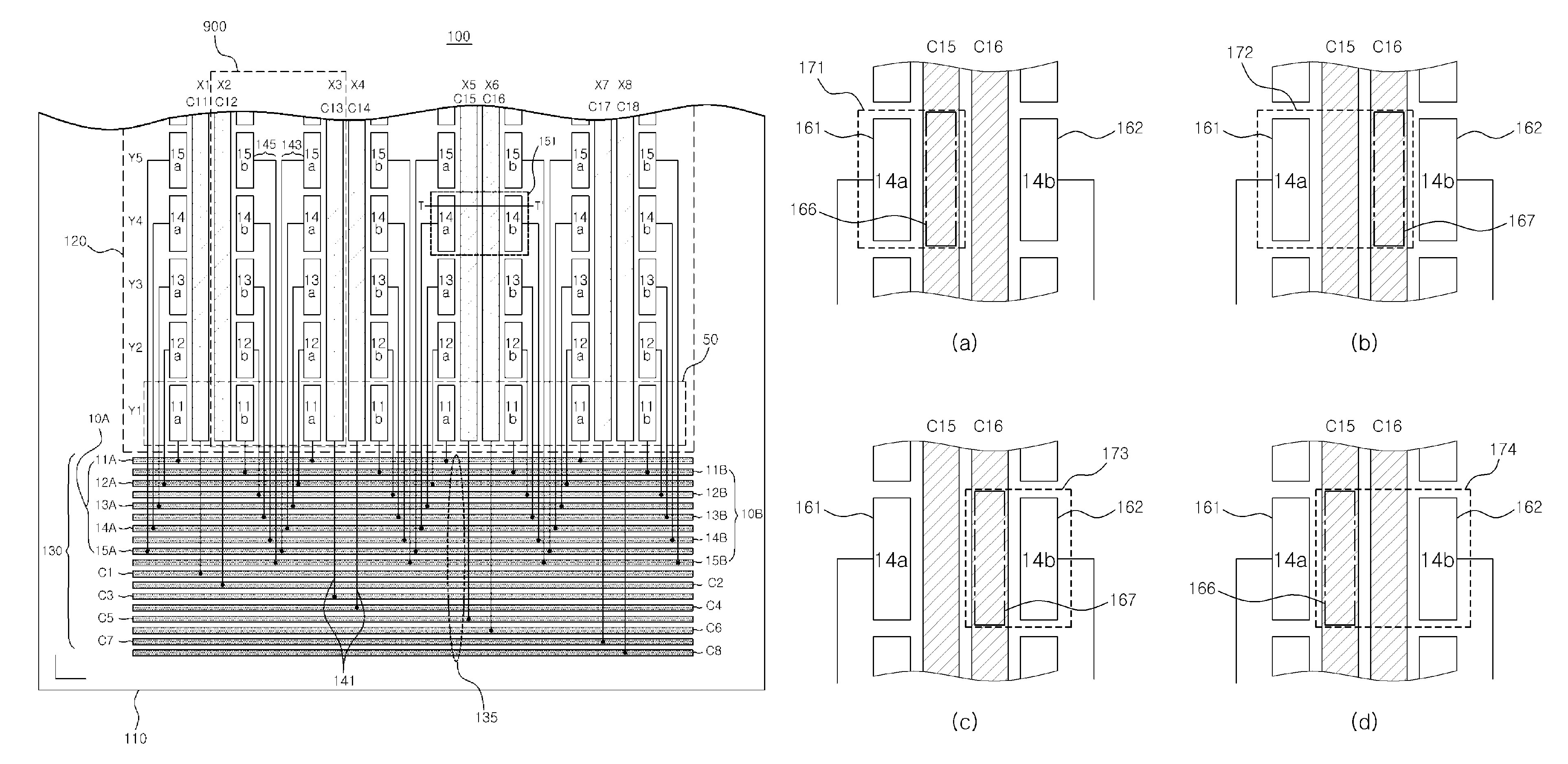
[0043]Exemplary embodiments are directed to a touch sensor panel for use in a touch sensor device such as, for example, a touchpad or a touch screen. For example, the touch sensor device may be a device capable of detecting a user's touch on a panel that is installed over a display screen or provided separately from the display screen. Information indicating whether there is a touch input detected from the panel or information indicating the location of the touch input may be used to control the operation of a computer system equipped with the touch sensor device or to manipulate data displayed on the screen of the computer system. The touch sensor panel may be installed or attached to a digital device such as, for example, a desktop personal computer (PC), a notebook computer, a tablet PC, a kiosk equipped with a large-scale display, a mobile communication terminal, a smart phone, a smart pad, a digital broadcast receiver, a personal digital assistant (PDA), a portable multimedia p...


PUM


Abstract

A touch sensor panel used for a display device is provided. The touch sensor panel can precisely determine a touch location with a given area of electrodes, can reduce the number of channels required, and can reduce the influence of noise. In addition, the touch sensor panel can improve sensing resolution with a given number of electrode channels, can be robust against noise, and can improve linearity by precisely determining a touch location and visibility of displayed image by dummy electrodes.

Description

CROSS-REFERENCE TO RELATED APPLICATIONS[0001]This application is a continuation of International Application No. PCT / KR2012 / 000292, filed Jan. 12, 2012, which claims priority to Korean Application Nos. 10-2011-0059814, filed on Jun. 20, 2011, and 10-2011-0066953 filed on Jul. 6, 2011, all of which hereby are incorporated by reference in their entirety for all purposes as if fully set forth herein.BACKGROUND OF THE INVENTION[0002]1. Field of the Invention[0003]The present invention relates to a touch sensor panel with improved touch sensitivity and a method of manufacturing the same, and more particularly, a touch sensor panel capable of precisely determining a touch location with a given area of electrodes, reducing the number of channels required, reducing the influence of noise and improving visibility of displayed image.[0004]2. Discussion of the Related Art[0005]With the widespread distribution of mobile phones equipped with touch screens and the commercialization of various typ...

Claims


Application Information

Patent Timeline
Patent Type & Authority Patents(United States)
IPC IPC(8): G06F3/044
CPCG06F3/044G06F2203/04101G06F2203/04104G06F3/0445G06F3/0446
Inventor KIM, JAE HONGOH, DO HWAN
Owner MELFAS
Why Eureka
Try Eureka