3D stacked non-volatile storage programming to conductive state

a non-volatile storage and programming technology, applied in digital storage, instruments, semiconductor devices, etc., can solve problems such as program disturbance and boosting voltage leakag

Active Publication Date: 2015-08-04
SANDISK TECH LLC
View PDF16 Cites 23 Cited by
  • Summary
  • Abstract
  • Description
  • Claims
  • Application Information

AI Technical Summary

Benefits of technology

[0170]One embodiment includes a 3D stacked non-volatile memory device, comprising a plurality of bit lines, a plurality of source lines, a plurality of word lines comprising conductive material that is oriented horizontally, a plurality of layers of dielectric material that alternates with the plurality of word lines in a stack; a plurality of NAND strings that are oriented vertically, and one or more managing circuits in communication with the plurality of word lines, the plurality of bit lines, the plurality of source lines, the drain side select gates, and the source side select gates. Each NAND string comprises a set of non-volatile storage elements, a drain side select gate at a first end of the NAND string, and a source side select gate at a second end of the NAND string. The drain side select gate of each NAND string is coupled to one of the bit lines. The source side select gate of each NAND string coupled to one of the source lines. The one or more managing circuits apply a select voltage to drain side select gates of a group of NAND strings of the plurality of NAND strings while applying a program voltage to selected bit lines associated with selected NAND strings of the group of NAND strings to pass the program voltage to channels of the respective selected NAND strings. The one or more managing circuits apply a first voltage to a selected word line associated with the group of NAND strings while the program voltage is in the channels of the selected NAND strings. The one or more managing circuits apply a second voltage to all unselected word lines associated with the selected NAND strings that are between the selected word line and the source select gates of the selected NAND strings while the program voltage is in the channels of the selected NAND strings to prevent programming of any non-volatile storage elements on the selected NAND strings that have already been programmed. The one or more managing circuits apply a third voltage to all unselected word lines associated with the selected NAND strings that are between the selected word line and the drain select gates of the selected NAND strings while the program voltage is in the channels of the selected NAND strings. The third voltage allows the program voltage to pass to channels of selected non-volatile storage elements and prevents programming of any non-volatile storage element on the selected NAND string between the selected word line and the drain side select gate.

Problems solved by technology

However, if the channel potential of an unselected NAND strings in a 3D stacked memory structure is boosted to inhibit programming, the boosting voltage could leak.
Leakage of the boosting voltage could result in program disturb.

Method used


Image

  • 3D stacked non-volatile storage programming to conductive state
  • 3D stacked non-volatile storage programming to conductive state
  • 3D stacked non-volatile storage programming to conductive state

Examples


Embodiment Construction

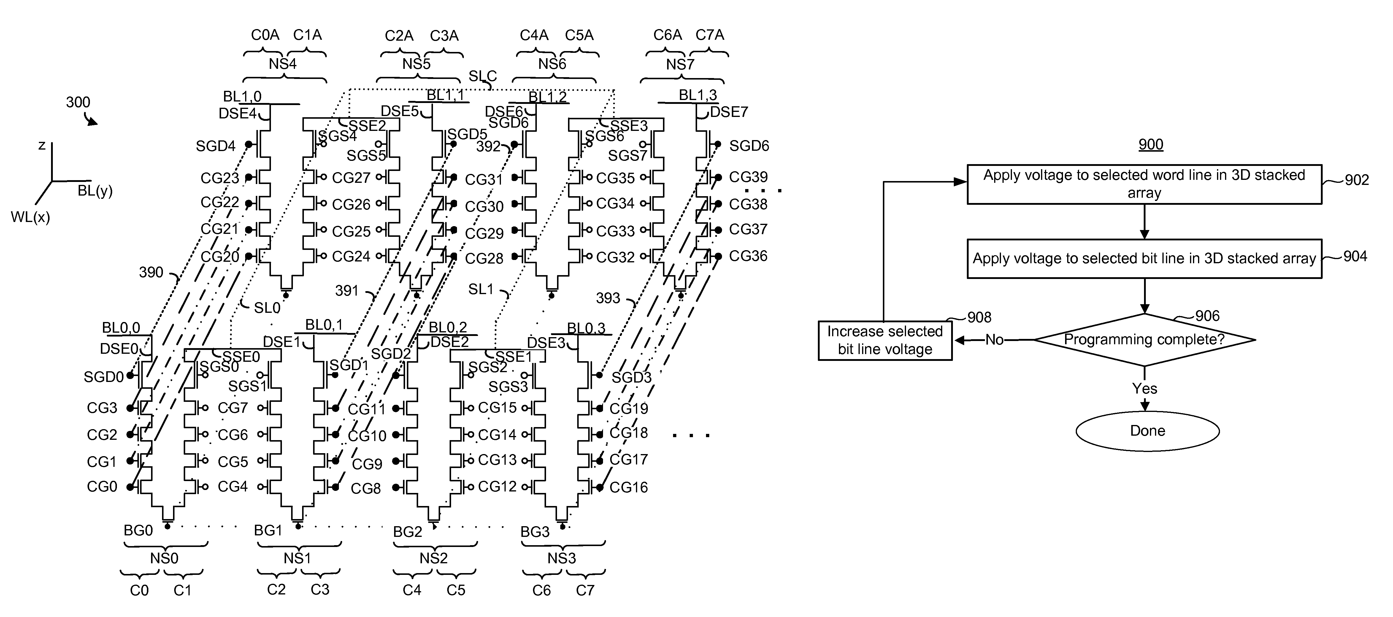
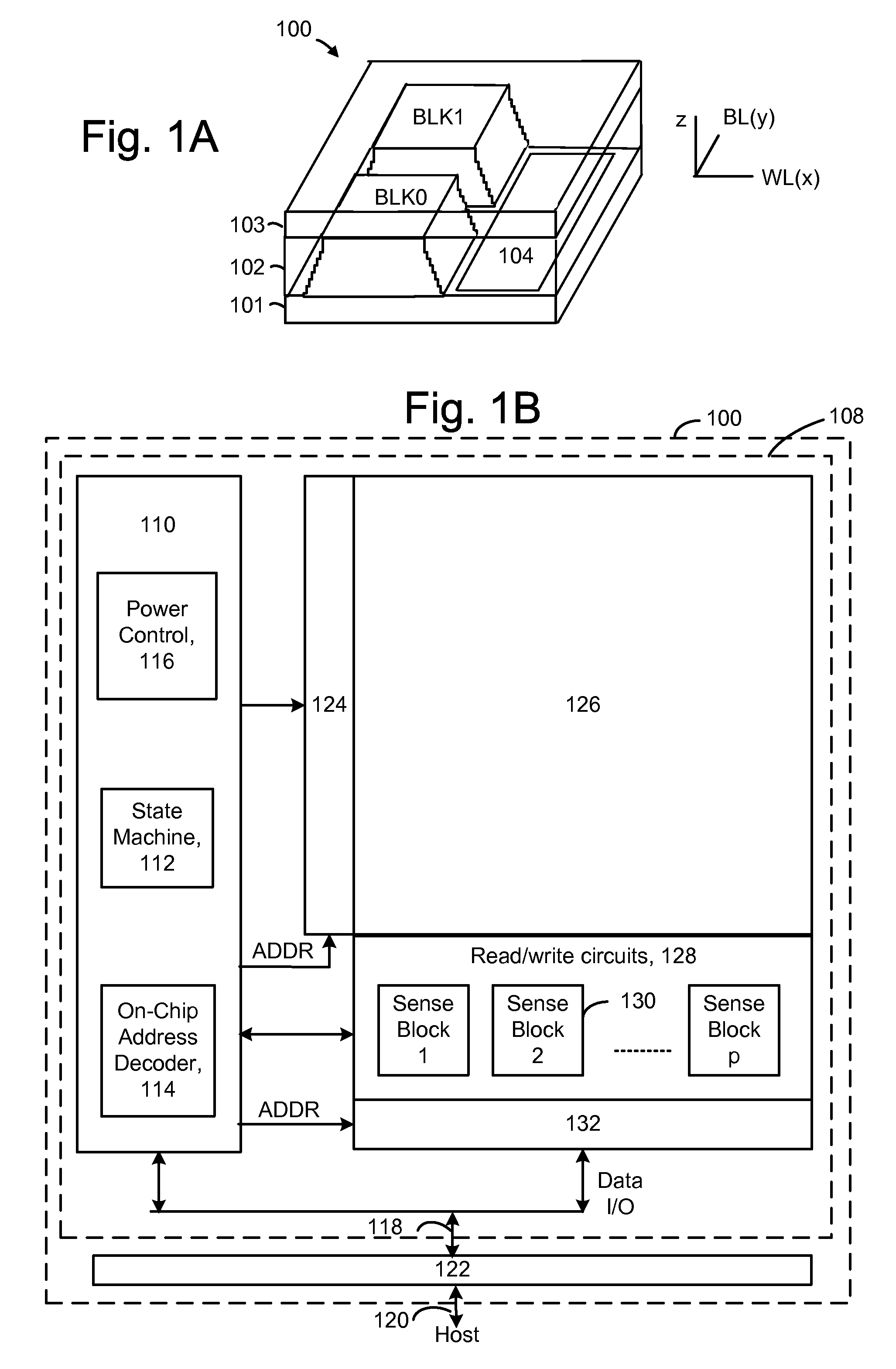
[0038]A 3D stacked non-volatile memory device can be arranged in multiple blocks. In one approach, the memory device includes NAND strings which have a drain-side select gate (SGD) transistor on one end and a source-side select gate (SGS) transistor on the other end.

[0039]One possible technique for programming the non-volatile storage elements in a 3D stacked memory device is to apply a program voltage to a gate of a selected non-volatile storage element while a lower voltage is in the channel below the selected non-volatile storage element. One possible technique to inhibit unselected NAND strings from programming is to boost the channel potential. However, the channel potential could leak, which may result in program disturb. NAND strings in some 3D stacked memory devices may be more susceptible to leakage of boosted channel potential than NAND strings in some 2D memory devices. A possible reason for this is that memory cells in a 3D stacked memory device may use a thin film trans...


PUM


Abstract

Programming NAND strings in a 3D stacked storage device to a conductive state. Storage elements may be erased by raising their Vt and programmed by lowering their Vt. Programming may include applying a series of increasing voltages to selected bit lines until the selected memory cell is programmed. Unselected bit lines may be held at about ground, or close to ground. The selected word line may be grounded, or be held close to ground. Unselected word lines between the selected word line and the bit line may receive about the selected bit line voltage. Unselected word lines between the source line and the selected word line may receive about half the selected bit line voltage. Programming may be achieved without boosting channels of unselected NAND strings to inhibit them from programming. Therefore, program disturb associated with leakage of boosted channel potential may be avoided.

Description

BACKGROUNDDescription of the Related Art[0001]Recently, ultra high density non-volatile storage devices have been proposed using a 3D stacked memory structure sometimes referred to as a Bit Cost Scalable (BiCS) architecture. For example, a 3D NAND stacked memory device can be formed from an array of alternating conductive and dielectric layers. A memory hole may be drilled in the layers to define many memory layers simultaneously. A NAND string may then be formed by filling the memory hole with appropriate materials. A straight NAND string extends in one memory hole, while a pipe- or U-shaped NAND string (P-BiCS) includes a pair of vertical columns of memory cells which extend in two memory holes and which are joined by a bottom back gate. Control gates of the memory cells are provided by the conductive layers.[0002]One possible technique for inhibiting an unselected NAND string from programming is to boost its channel potential. However, if the channel potential of an unselected NA...

Claims


Application Information

Patent Timeline
Patent Type & Authority Patents(United States)
IPC IPC(8): G11C11/56G11C16/10H01L27/11G11C16/04H01L27/115
CPCG11C11/5671G11C16/10H01L27/11582H01L27/1157G11C16/0483H10B43/35H10B43/27
Inventor MIHNEA, ANDREICOSTA, XIYINGZHANG, YANLI
Owner SANDISK TECH LLC
Why Eureka
Try Eureka