Nanowire sensor having nanowire of network structure

a network structure and nanowire technology, applied in the field of nanowire sensors, can solve the problems of nanowires having a smaller thickness than bottom-up type nanowires, nanowires may be bent or collapsed, and achieve the effect of improving measurement sensitivity and increasing the probability of a detection material being attached

Active Publication Date: 2015-08-04
POSTECH ACAD IND FOUND
View PDF15 Cites 0 Cited by
  • Summary
  • Abstract
  • Description
  • Claims
  • Application Information

AI Technical Summary

Benefits of technology

[0013]Accordingly, the present invention has been made in an effort to solve the problems occurring in the related art, and an object of the present invention is to provide a nanowire sensor which includes a nanowire formed in a network structure so as to have a larger exposed surface area than a nanowire sensor including a straight nanowire, thereby increasing the probability that a detection material will be attached to the nanowire and improving measurement sensitivity.

Problems solved by technology

At this time, since the nanowires are not easily synthesized and aligned, there are difficulties in mass-producing the nanowire sensor.
In the case of the top-down type nanowire fabricated through a silicon-on insulator (SOI) substrate, an excellent electric characteristic may be obtained, but there are difficulties in implementing a nanowire having a smaller thickness than the bottom-up type nanowire due to the limit of exposure technology.
Furthermore, when a gate-all-around device is implemented to acquire a high sensitivity, nanowires may be bent or collapse in case where the nanowires have a length of several hundred nm or more.
Furthermore, the top-down type nanowire is structurally unstable for a flow of fluid.
Thus, the number of elements with respect to area may be decreased to thereby make it difficult to reduce a cost.

Method used


Image

  • Nanowire sensor having nanowire of network structure
  • Nanowire sensor having nanowire of network structure
  • Nanowire sensor having nanowire of network structure

Examples


Embodiment Construction

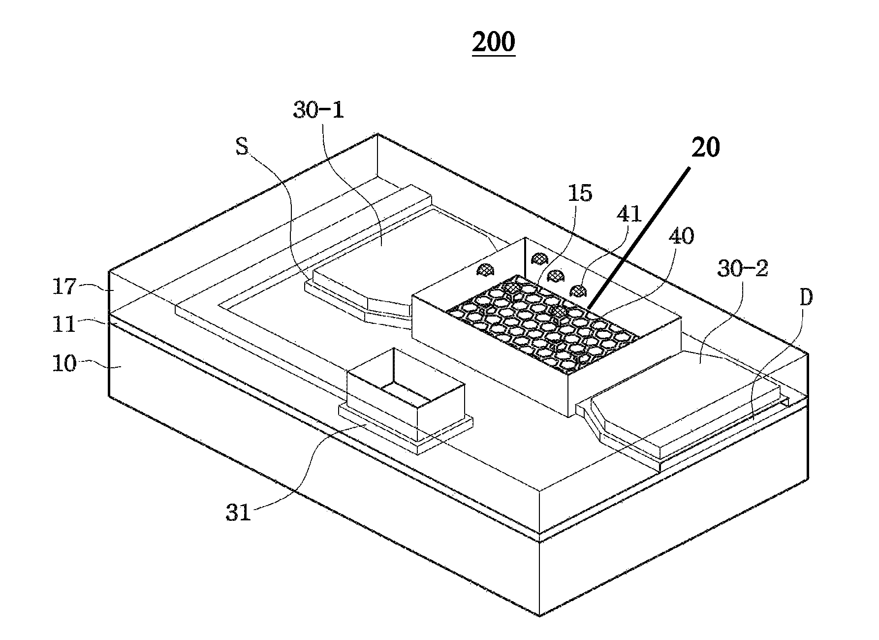
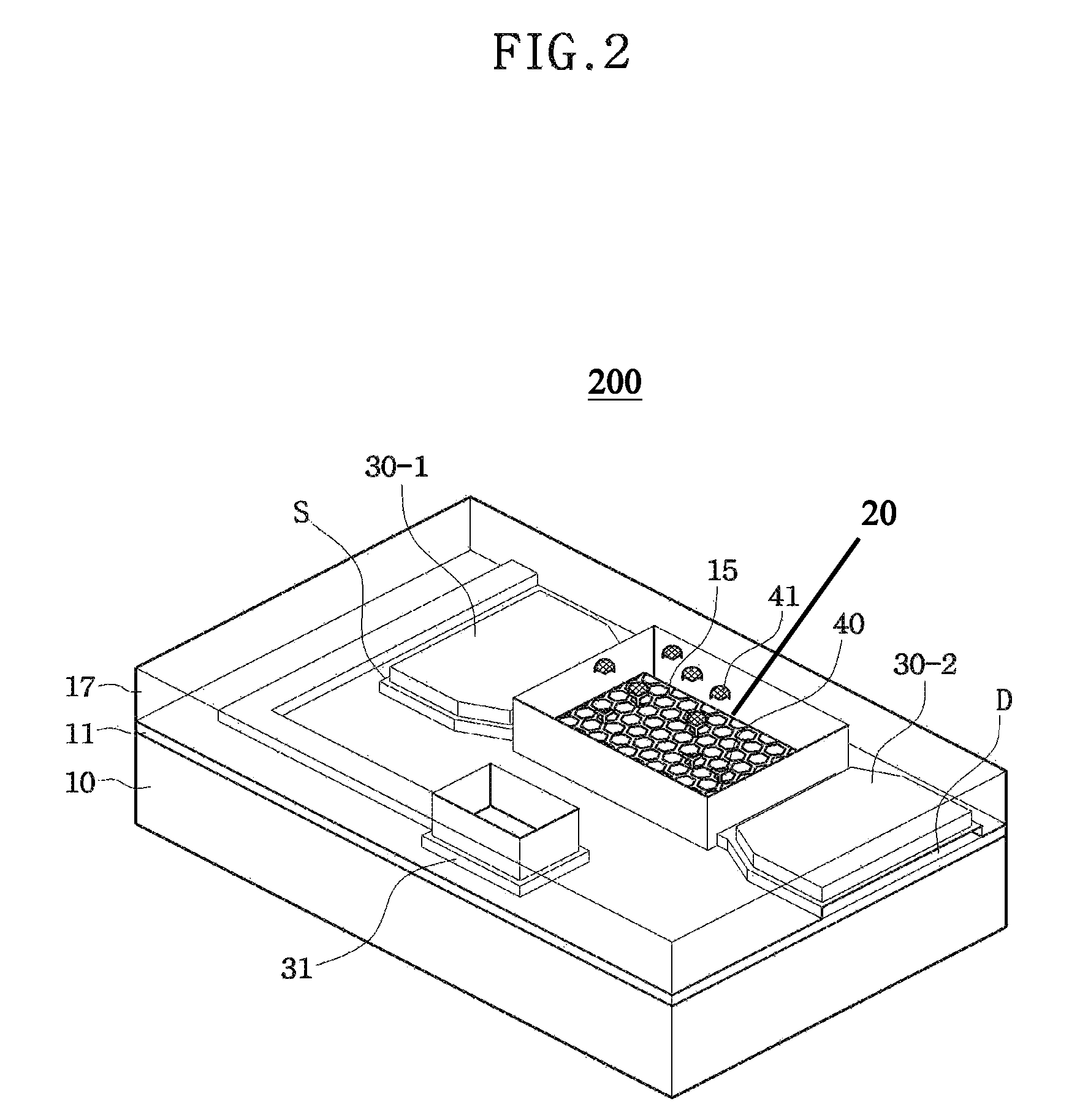
[0023]Reference will now be made in greater detail to a preferred embodiment of the invention, an example of which is illustrated in the accompanying drawings. Wherever possible, the same reference numerals will be used throughout the drawings and the description to refer to the same or like parts.

[0024]FIG. 2 is a diagram for explaining the structure and operation principle of a nanowire sensor having a nanowire in a network structure according to an embodiment of the present invention.

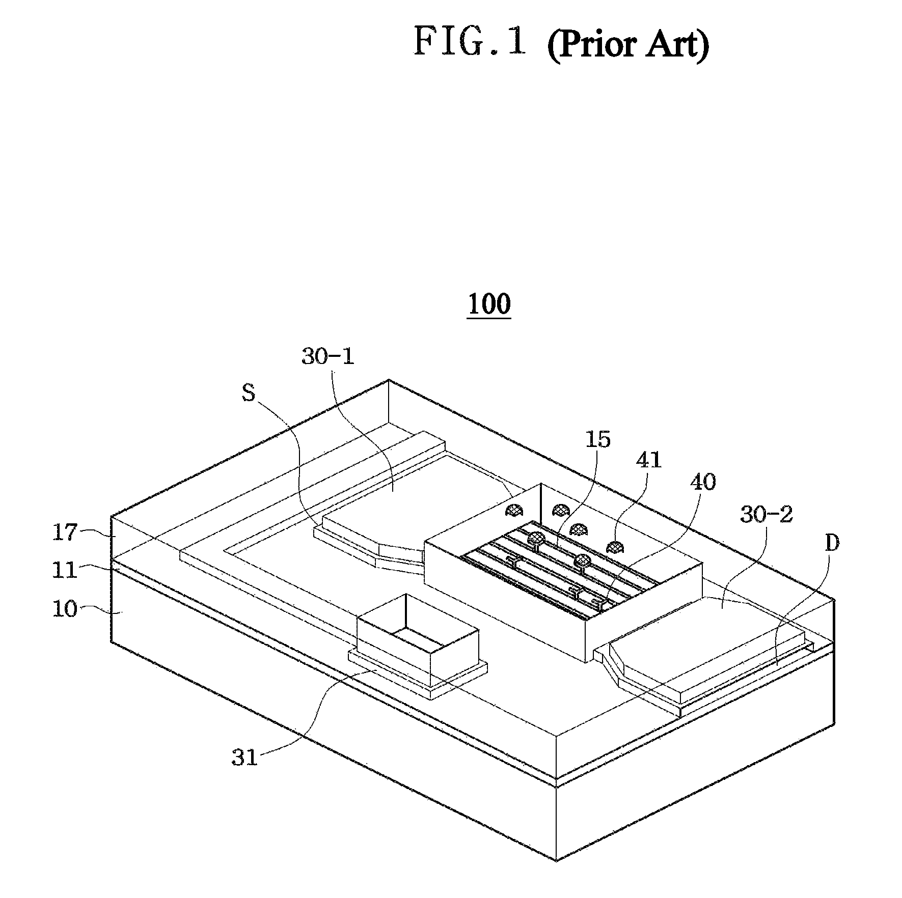
[0025]Referring to FIG. 2, the nanowire sensor 200 having a nanowire in a network grid structure according to the embodiment of the present invention includes a source electrode 30-1 and drain electrode 30-2 formed over a substrate, a nanowire grid 20 formed between the source electrode 30-1 and the drain electrode 30-2 and having a network structure in which patterns of intersections are repeated, and a detection material 40 fixed to the nanowire and selectively responding to a target material intro...


PUM

PropertyMeasurementUnit
widthaaaaaaaaaa
lengthaaaaaaaaaa
semiconductoraaaaaaaaaa

Abstract

A nanowire sensor having a nanowire in a network structure includes: source and drain electrodes formed over a substrate; a nanowire formed between the source and drain electrodes and having a network structure in which patterns of intersections are repeated; and a detection material fixed to the nanowire and selectively reacting with a target material introduced from outside.

Description

BACKGROUND OF THE INVENTION[0001]1. Field of the Invention[0002]The present invention relates to a nanowire sensor using a nanowire, and more particularly, to a nanowire sensor having a nanowire in a network structure, which uses a nanowire in a network structure including repeated patterns instead of a straight nanowire, thereby obtaining high efficiency and structural stability.[0003]2. Description of the Related Art[0004]An electrochemical sensor is an element which converts a physical or chemical characteristic of a target material into an electrical signal. The electrochemical sensor is expected to be widely used as a biosensor, chemical sensor or environmental sensor, depending on a target material.[0005]In order to sense and analyze a target material using an electrochemical sensor, the electrochemical sensor must have such a high sensitivity that a signal is significantly changed for a fine characteristic of the target material. Furthermore, the electrochemical sensor must h...

Claims


Application Information

Patent Timeline
Patent Type & Authority Patents(United States)
IPC IPC(8): H01L27/14H01L29/66G01N27/327G01N33/487G01N27/06H01L21/00H01L29/775B82Y40/00
CPCG01N27/06G01N27/3278G01N33/48707H01L29/66477H01L29/775B82Y40/00B82B1/00G01N27/30G01N27/406
Inventor LEE, JEONG SOOJEONG, YOON HARIM, TAI UKBAEK, CHANG KIKIM, SUNG HOKIM, KI HYUN
Owner POSTECH ACAD IND FOUND
Why Eureka
Try Eureka