Semiconductor device with integrated magnetic element provided with a barrier structure against metal contamination, and manufacturing

a technology of magnetic element and barrier structure, which is applied in the direction of semiconductor devices, magnetic measurements, instruments, etc., can solve the problems of not always usable, etching proves to be invasive, and does not guarantee the elimination of contaminants

Active Publication Date: 2015-08-11
STMICROELECTRONICS SRL
View PDF8 Cites 3 Cited by
  • Summary
  • Abstract
  • Description
  • Claims
  • Application Information

AI Technical Summary

Problems solved by technology

However, it is evident that an analysis by means of XRF spectroscopy is a method control, and not prevention, of contamination.
Likewise, removal of metal contaminants by etching proves to be an invasive technique, which is not always usable and does not guarantee a complete elimination of the contaminants.
The steps of FIGS. 2-6 entail a risk of contamination of the wafer and / or of the manufacturing equipment used during said step.
A possible solution could include the step of providing the intermediate layer 2 with a large thickness, but this would render more complex the provision of possible deep vias through the intermediate layer 2, in addition to increasing the thickness of the wafer 10 in an undesirable way.
The contamination deriving from metal ions may jeopardize even significantly operation of the electronic devices 9 in so far as undesirable metal ions concur in modifying the characteristics of conductivity of the regions in which they are present.
Also the step of FIG. 4, where the magnetic layer 3 is removed selectively by wet etching or dry etching, may entail a contamination of the etching equipment.
Also this step may lead to a contamination of the etching equipment owing to removal of the mask 4, in so far as the magnetic layer 3 is exposed at the end of etching of the mask 4.
It is evident from the description of the steps of FIGS. 2-6 that the risks of contamination of the wafer 10 and / or of the equipment used for manufacture thereof are multiple and can be difficult to control.
Detection of the contamination of the equipment leads to suspension of use thereof awaiting a thorough cleaning step, with consequent obvious disadvantages.
In fact, ferromagnetic materials generally contain iron, nickel, cobalt, and other contaminating elements, which, in some cases, may lead to the failure of the electronic components 9 integrated in the wafer 10.
The more technological steps are carried out after deposition of the ferromagnetic material, the greater the number of items of equipment that are used just for machining the wafers with the magnetic sensors, and the higher the costs involved.

Method used


Image

  • Semiconductor device with integrated magnetic element provided with a barrier structure against metal contamination, and manufacturing
  • Semiconductor device with integrated magnetic element provided with a barrier structure against metal contamination, and manufacturing
  • Semiconductor device with integrated magnetic element provided with a barrier structure against metal contamination, and manufacturing

Examples


Embodiment Construction

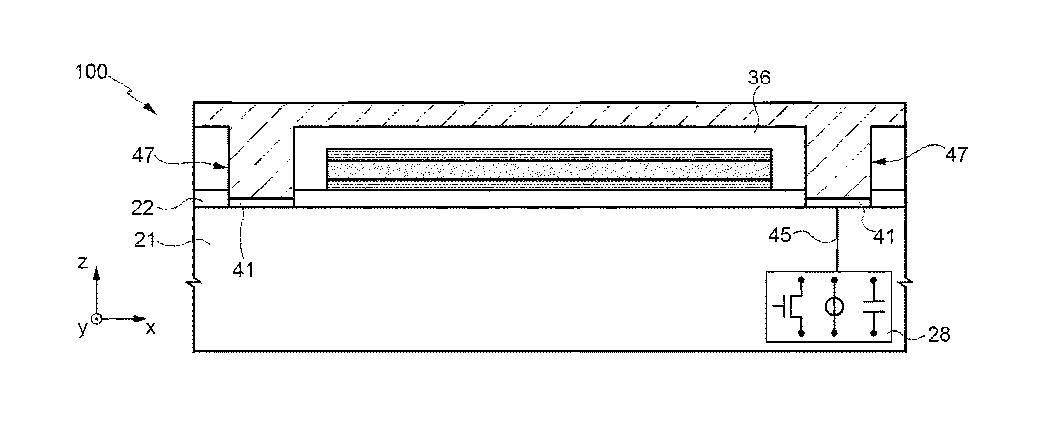
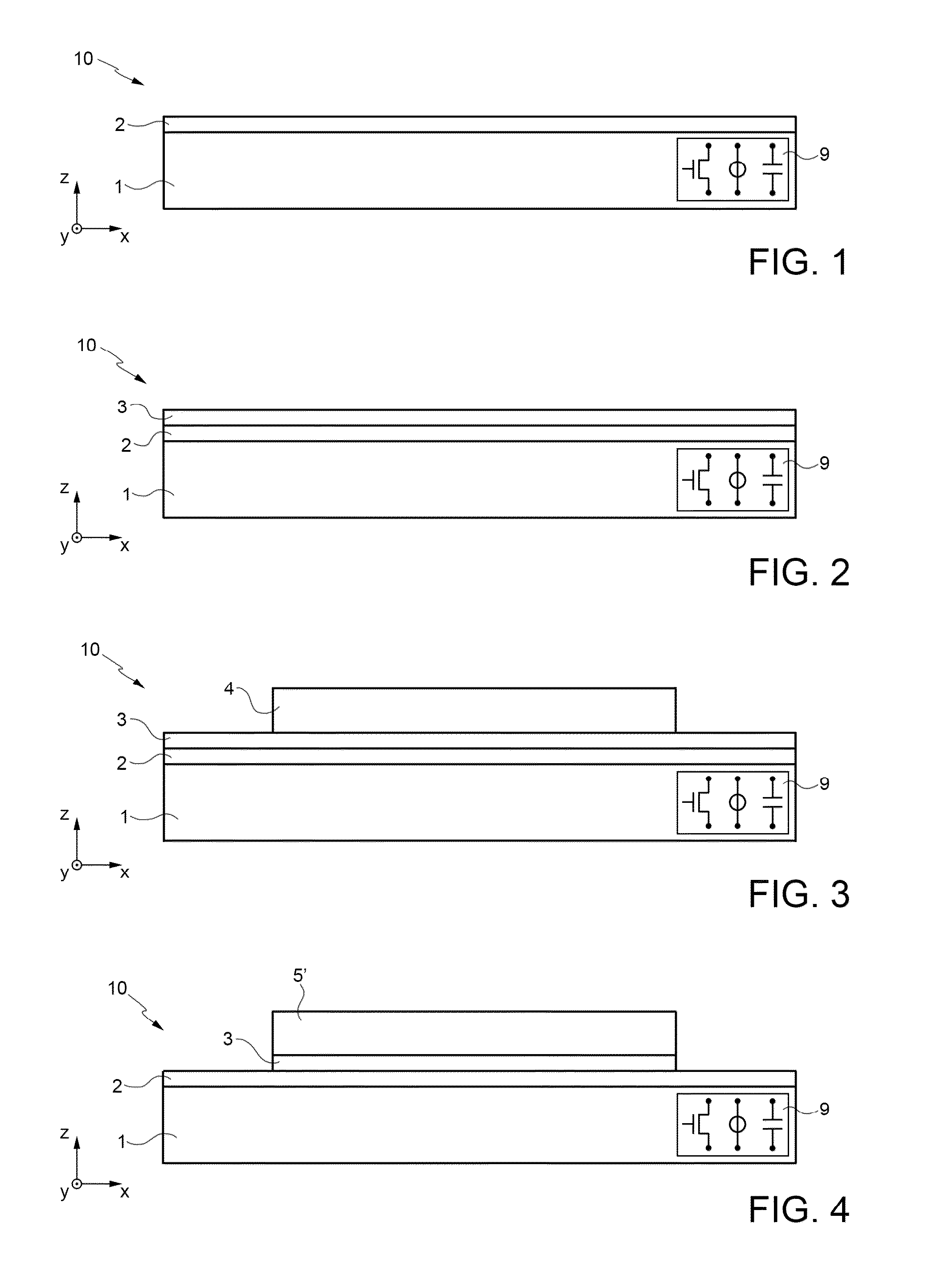
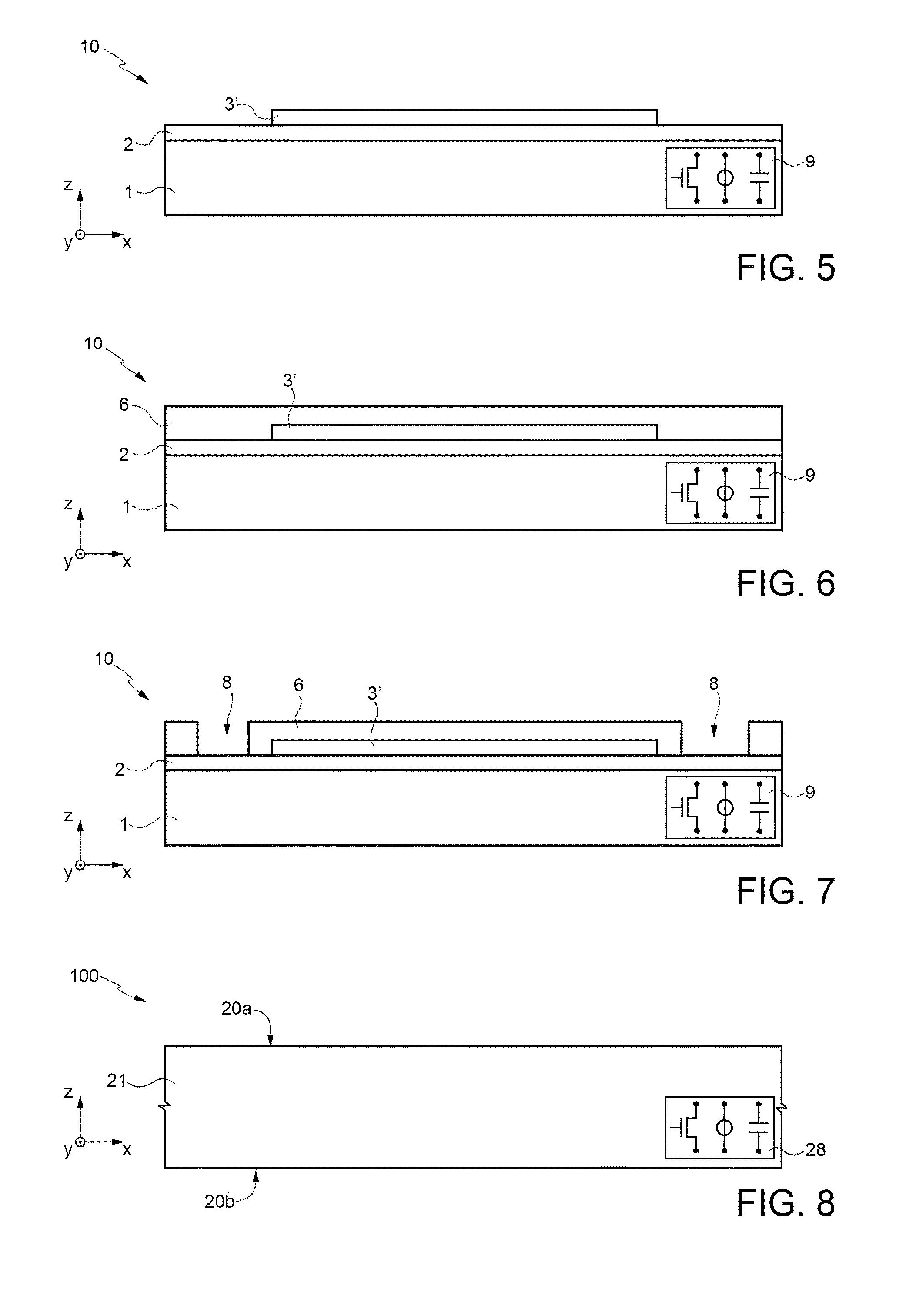
[0062]Provided according to the embodiments is a semiconductor device comprising: a semiconductor body, having a first side and a second side opposite to one another; a first barrier element, which extends over the first side of the semiconductor body and is made of a first material configured to act as barrier against metal ions, for example chosen from among titanium, tantalum, titanium alloy, including TiN and TiW, tantalum alloy, including TaNTa and TaN; a magnetic element, which extends over the first barrier layer and is made of a second material having magnetic properties, for example a ferromagnetic material, in particular chosen from among CoZrTa, NiFe, CoFeHfO, CoFeSiB, CoZrO; a second barrier element, which extends over the magnetic layer and is made of a third material configured to act as barrier against metal ions, for example chosen from among titanium, tantalum, titanium alloy, including TiN and TiW, tantalum alloy, including TaNTa and TaN. The first and second barri...


PUM

PropertyMeasurementUnit
thicknessaaaaaaaaaa
thicknessaaaaaaaaaa
thicknessaaaaaaaaaa

Abstract

A semiconductor device including: a semiconductor body having a first side and a second side opposite to one another; a first barrier element, which extends over the first side of the semiconductor body and is made of a first material configured to act as barrier against metal ions, for example chosen from among titanium, tantalum, titanium alloys or compounds, tantalum alloy; a magnetic element, which extends over the first barrier layer and is made of a second material having magnetic properties, for example a ferromagnetic material; a second barrier element, which extends over the magnetic layer and is made of a third material configured to act as barrier against metal ions, for example chosen from among titanium, tantalum, titanium alloys or compounds, tantalum alloys or compounds. The first and second barrier elements form a top encapsulating structure and a bottom encapsulating structure for the magnetic element.

Description

CROSS REFERENCE TO RELATED APPLICATION[0001]This application claims priority to Italian Patent Application No. TO2012A001080, filed Dec. 14, 2012, which is hereby incorporated by reference to the maximum extent allowable by law.BACKGROUND[0002]1. Technical Field[0003]The present disclosure relates to a semiconductor device having an integrated magnetic element and provided with a barrier structure against metal contamination, and to a method for manufacturing the semiconductor device. In particular, the semiconductor device includes a magnetic element and the barrier structure is designed to protect, during the manufacturing steps of the semiconductor device, the semiconductor device itself from metal contamination deriving from formation of the magnetic element. Moreover, the barrier structure also protects from metal contamination the equipment used during the steps of manufacturing the semiconductor device.[0004]2. Discussion of the Related Art[0005]In processes of micromachining...

Claims


Application Information

Patent Timeline
Patent Type & Authority Patents(United States)
IPC IPC(8): H01L27/22H01L43/14G01R33/00H01L43/04H01L27/06
CPCG01R33/0052H01L27/22H01L43/14H01L43/04H01L27/0688H10B61/00H10N59/00H10N52/80H10N52/01
Inventor IULIANO, PAOLOMILANESI, FRANCESCAPALUMBOPIROTTA, SONIA
Owner STMICROELECTRONICS SRL
Why Eureka
Try Eureka