Silicide protection during contact metallization and resulting semiconductor structures

a technology of contact metallization and silicide protection, which is applied in the direction of semiconductor devices, semiconductor/solid-state device details, electrical devices, etc., can solve the problems of polymeric etch residue formation and degradation of the performance of the semiconductor device, and achieve the effect of preventing damage to silicid

Active Publication Date: 2015-08-18
GLOBALFOUNDRIES U S INC
View PDF5 Cites 167 Cited by
  • Summary
  • Abstract
  • Description
  • Claims
  • Application Information

AI Technical Summary

Benefits of technology

[0007]The shortcomings of the prior art are overcome and additional advantages are provided through the provision, in one aspect, of a method of preventing damage to silicide during contact metallization. The method includes providing a semiconductor structure for a transistor, the structure including a metal gate coupled to a channel region and a spacer of protective material on either side of the metal gate. The method further includes creating a first layer of protective material over a source region and a drain region of the transistor, and creating a second layer of protective material over the gate, the first protective layer acting as an etch stop for creating intermediate openings to the source region and drain region, and the first and second protective layers being configured to allow punch-through of the first protective layer while preventing etching through the second protective layer. The method further includes creating silicide in the source region and the drain region after creating an intermediate gate opening and prior to fully etching a gate opening.

Problems solved by technology

The use of oxygen plasma results in the formation of polymeric etch residues at the bottom of contact openings in source, drain and gate regions of the semiconductor device.
However, the oxygen plasma ash processes and other prior art processes cause damage to the exposed silicide and increase the resistance of the subsequent contact metallization, resulting in degradation of the performance of the semiconductor device.

Method used


Image

  • Silicide protection during contact metallization and resulting semiconductor structures
  • Silicide protection during contact metallization and resulting semiconductor structures
  • Silicide protection during contact metallization and resulting semiconductor structures

Examples


Embodiment Construction

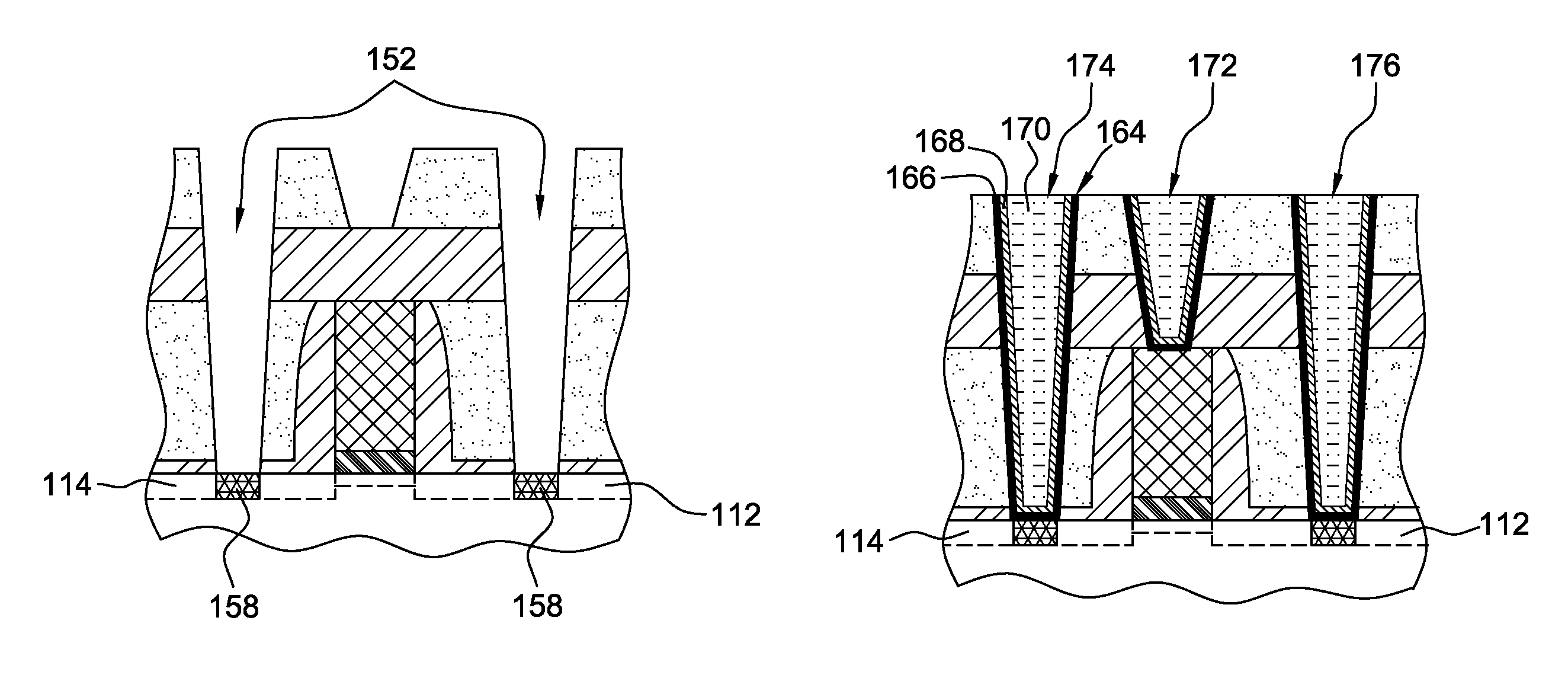
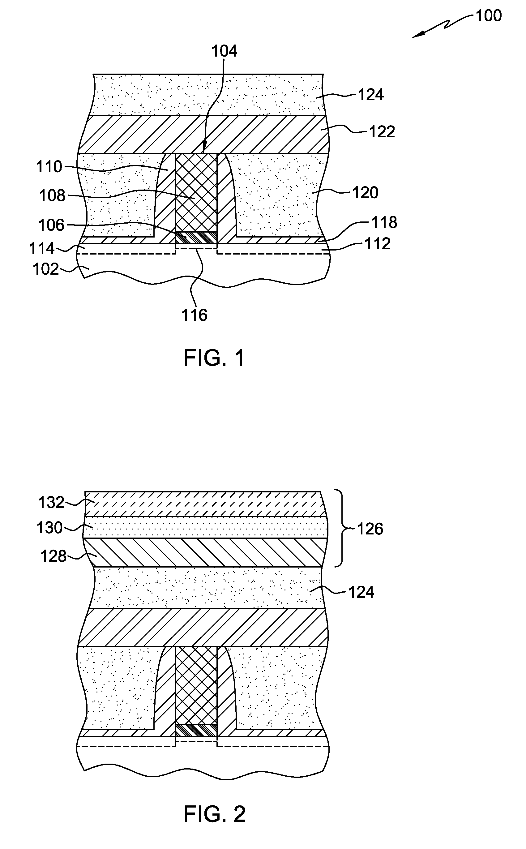
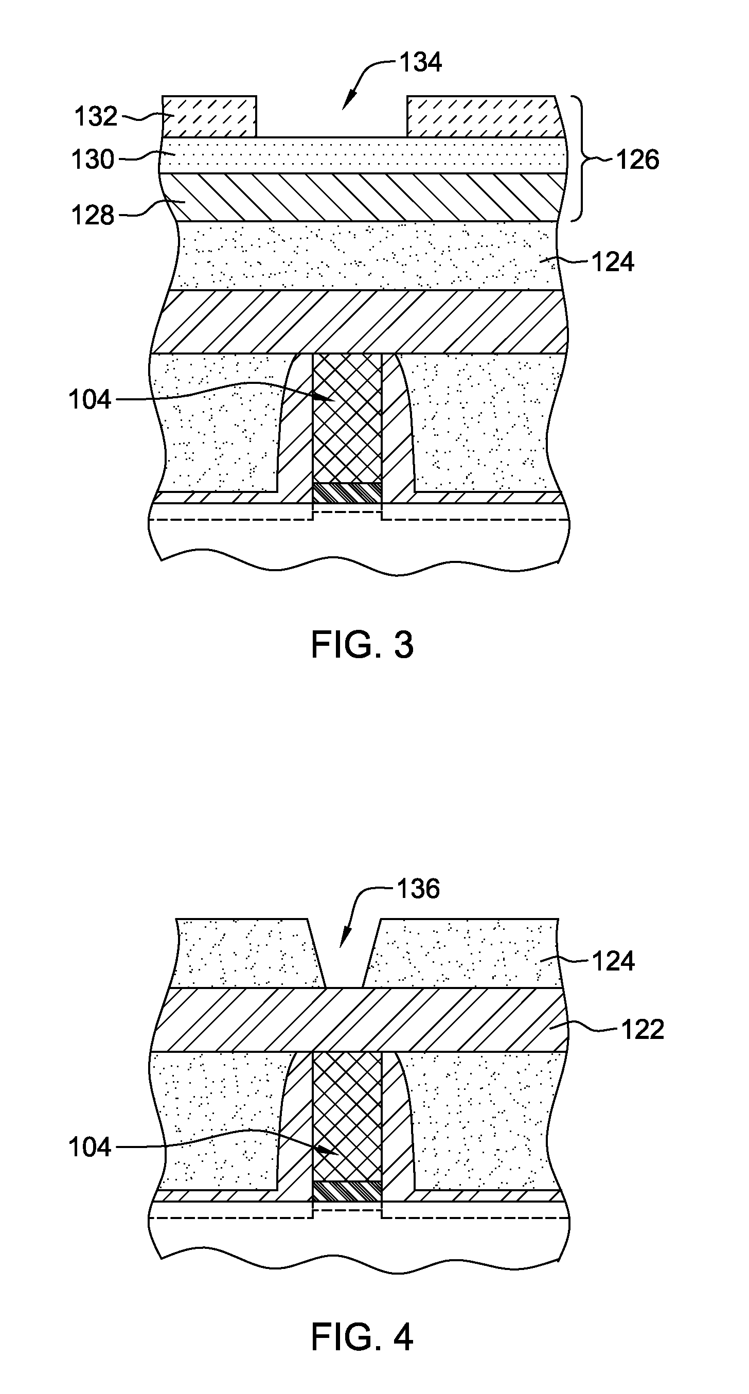
[0030]Aspects of the present invention and certain features, advantages, and details thereof, are explained more fully below with reference to the non-limiting examples illustrated in the accompanying drawings. Descriptions of well-known materials, fabrication tools, processing techniques, etc., are omitted so as not to unnecessarily obscure the invention in detail. It should be understood, however, that the detailed description and the specific examples, while indicating aspects of the invention, are given by way of illustration only, and are not by way of limitation. Various substitutions, modifications, additions, and / or arrangements, within the spirit and / or scope of the underlying inventive concepts will be apparent to those skilled in the art from this disclosure.

[0031]Approximating language, as used herein throughout the specification and claims, may be applied to modify any quantitative representation that could permissibly vary without resulting in a change in the basic fun...


PUM

PropertyMeasurementUnit
dielectric constantaaaaaaaaaa
thicknessaaaaaaaaaa
thicknessaaaaaaaaaa

Abstract

A semiconductor transistor has a structure including a semiconductor substrate, a source region, a drain region and a channel region in between the source region and the drain region. A metal gate, having a top conductive portion of tungsten is provided above the channel region. A first silicon nitride protective layer over the source region and the drain region and a second silicon nitride protective layer over the gate region are provided. The first silicon nitride protective layer and the second silicon nitride protective layer are configured to allow punch-through of the first silicon nitride protective layer while preventing etching through the second silicon nitride protective layer. Source and drain silicide is protected by avoiding fully etching a gate opening unless either the etching used would not harm the silicide, or the silicide and source and drain contacts are created prior to fully etching an opening to the gate for a gate contact.

Description

BACKGROUND OF THE INVENTION[0001]1. Technical Field[0002]The present invention generally relates to semiconductor devices and methods of fabricating semiconductor devices. More particularly, the present invention relates to preventing damage to silicide in transistor fabrication during non-self-aligned contact metallization.[0003]2. Background Information[0004]Silicide processes have been widely used to form silicide contacts on gate regions and source / drain regions during the semiconductor device fabrication processing to improve the performance of the semiconductor device. The silicide layer improves the operational speed of the semiconductor device by reducing the contact resistance between the metal contact and the source, drain and gate regions.[0005]In a typical semiconductor fabrication processing, one or more etching processes are performed simultaneously using a photoresist mask, to selectively form contacts over the silicide in source, drain and gate regions of the semicon...

Claims


Application Information

Patent Timeline
Patent Type & Authority Patents(United States)
IPC IPC(8): H01L21/8234H01L21/28H01L29/417H01L21/285H01L29/66H01L29/78
CPCH01L29/41791H01L21/28518H01L29/66795H01L29/785H01L2924/0002H01L23/485H01L23/53223H01L23/53238H01L23/53266H01L21/76816H01L21/76843H01L21/76855H01L21/76877H01L2924/00H01L23/535H01L29/456H01L29/495H01L29/7851
Inventor KAMINENI, VIMAL K.XIE, RUILONGMILLER, ROBERT
Owner GLOBALFOUNDRIES U S INC
Why Eureka
Try Eureka