Check patentability & draft patents in minutes with Patsnap Eureka AI!

Light emitting diode display device

a technology of light-emitting diodes and display devices, which is applied in the direction of instruments, static indicating devices, etc., can solve the problems of many restrictions in manufacturing a panel having high resolution and inevitable increase in pixel siz

Active Publication Date: 2015-09-08
LG DISPLAY CO LTD
View PDF19 Cites 2 Cited by
  • Summary
  • Abstract
  • Description
  • Claims
  • Application Information

AI Technical Summary

Benefits of technology

The patent is about a new LED display device that reduces the space taken up by each pixel, making it easier to create high-resolution and high-definition display panels. The device works by sharing a common capacitor between two pixels. The technical effect is a more efficient use of space, resulting in a more compact and visually appealing display.

Problems solved by technology

As a result, pixel size is inevitably increased.
This causes many restrictions in manufacturing a panel having high resolution.

Method used


Image

  • Light emitting diode display device
  • Light emitting diode display device
  • Light emitting diode display device

Examples


Embodiment Construction

[0019]Reference will now be made in detail to the preferred embodiments of the present invention, examples of which are illustrated in the accompanying drawings.

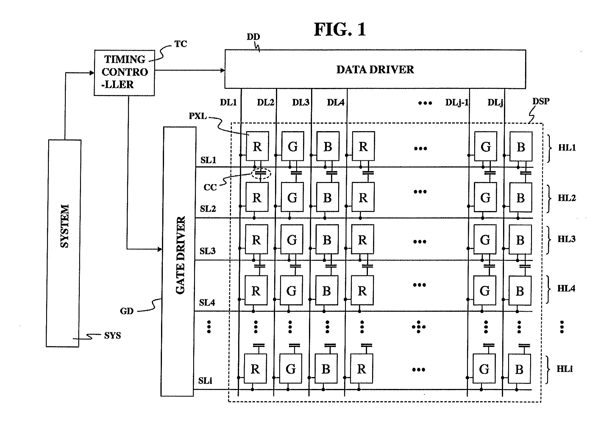
[0020]FIG. 1 is a diagram illustrating a light emitting diode (LED) display device according to an exemplary embodiment of the present invention.

[0021]As illustrated in FIG. 1, the LED display device according to the illustrated embodiment of the present invention includes a display panel (DSP), a system SYS, a gate driver GD, a data driver DD, and a timing controller TC.

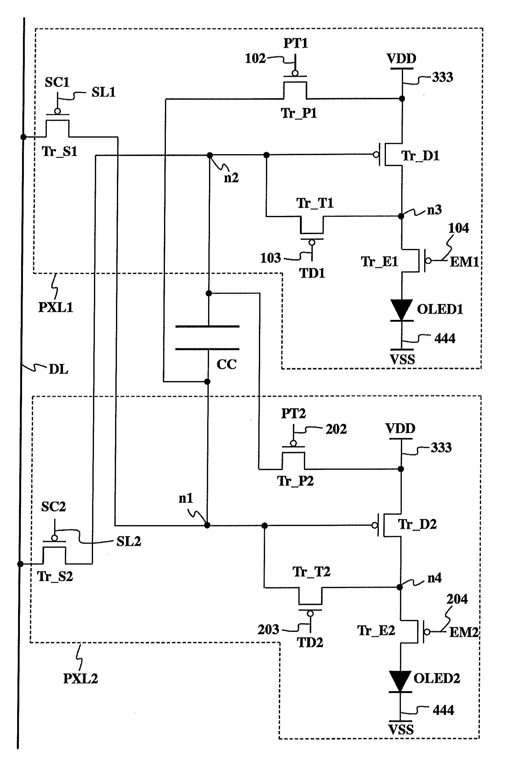
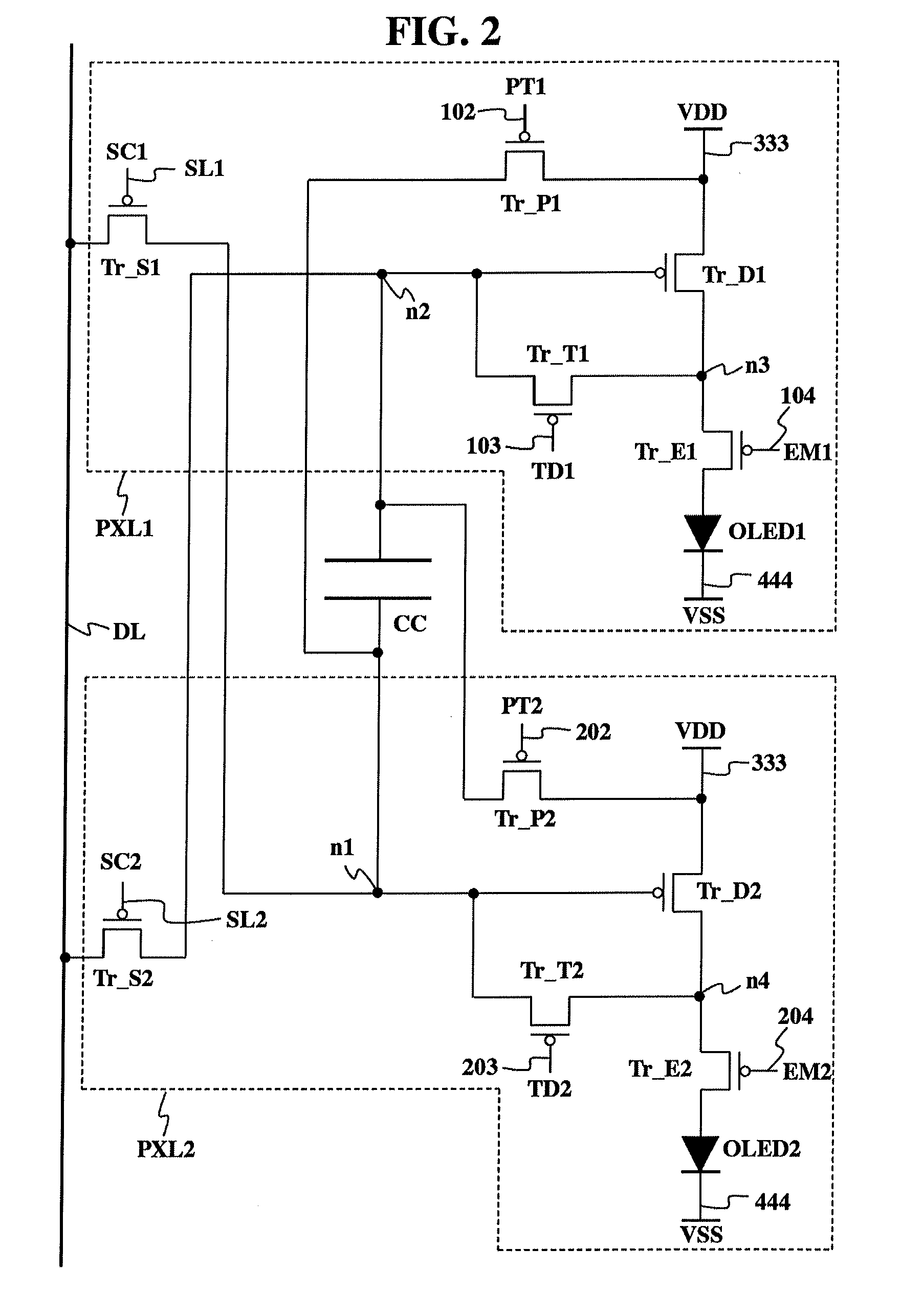
[0022]The display panel DSP includes a plurality of pixels PXL, i scan lines SL1 to SLi (i is a natural number greater than 1), and j data lines DL1 to DLj (j is a natural number greater than 1).

[0023]The pixels PXL are arranged in the form of a matrix array on the display panel DSP. The pixels PXL are classified into red pixels PXL to display red, green pixels PXL to display green and blue pixels PXL to display blue. Three horizontally adjacent pixels, whic...


PUM


Abstract

An LED display device includes a first scan switching element between a data line and a first node, a first voltage transfer switching element between a first drive voltage line and the first node, a first detection switching element between second and third nodes, a first driving switching element between the first drive voltage line and the third node, a first emission control switching element between the third node and a first LED, a second scan switching element between the data line and the second node, a second voltage transfer switching element between the first drive voltage line and the second node, a second detection switching element between the first node and a fourth node, a second driving switching element, a second emission control switching element between the fourth node and a second LED, and a common capacitor between the first node and the second node.

Description

[0001]This application claims the benefit of priority to Korean Patent Application No. 10-2012-0149852 filed on Dec. 20, 2012 which is hereby incorporated by reference as if fully set forth herein.BACKGROUND[0002]1. Field of the Disclosure[0003]The present disclosure relates to a light emitting diode (LED) display device, and, more particularly, to an LED display device in which two pixels share one common capacitor, to reduce the area occupied by each pixel, thereby being capable of facilitating manufacture of a display panel having high resolution and high definition.[0004]2. Discussion of the Related Art[0005]Pixels of an LED display device each includes a driving switching element, which is a current regulating element. The current driving capability of such a driving switching element is greatly influenced by the threshold voltage of the driving switching element. For this reason, it is important to correct current driving capability deviation among driving switching elements o...

Claims


Application Information

Patent Timeline
Patent Type & Authority Patents(United States)
IPC IPC(8): G09G3/32
CPCG09G3/32G09G3/3233G09G2300/0465G09G2300/0814G09G2300/0819G09G2300/0842G09G2300/0861G09G2300/0809G09G3/30
Inventor LEE, JAE-MYONCHO, NAM-WOOK
Owner LG DISPLAY CO LTD
Features
  • R&D
  • Intellectual Property
  • Life Sciences
  • Materials
  • Tech Scout
  • Unparalleled Data Quality
  • Higher Quality Content
  • 60% Fewer Hallucinations
Learn More