Liquid crystal display device

a liquid crystal display and display panel technology, applied in non-linear optics, instruments, optics, etc., can solve the problems of hardly ensuring a consistent strength, insufficient measurement accuracy, and varied bending strength of finished liquid crystal display panels, so as to achieve efficient and accurate evaluation of conditions and reliably high quality

Active Publication Date: 2015-11-24
JAPAN DISPLAY INC
View PDF11 Cites 0 Cited by
  • Summary
  • Abstract
  • Description
  • Claims
  • Application Information

AI Technical Summary

Benefits of technology

[0009]It is an object of the present invention to achieve a liquid crystal display device that enables an efficient and accurate evaluation of the bending strength in the production line. It is another object of the present invention to achieve a liquid crystal display device having consistent bending strength characteristics.
[0013]According to the present invention, it is possible to efficiently and accurately evaluate a condition, such as a chip, of a glass substrate constituting a liquid crystal display panel. Furthermore, because the total number of the liquid crystal display panels can be evaluated in a short time, it is possible to perform the evaluation of the bending strength on the total number of liquid crystal display panels and also to provide the market with the liquid crystal display panels having a reliably high quality.

Problems solved by technology

Chamfering the glass substrate such as the TFT substrate and the opposing substrate constituting the liquid crystal display panel may improve the bending strength, but hardly ensures a consistent strength.
Although it is performed on and near the chamfered edge of the glass substrate using an optical system such as a camera, the measurement accuracy has not been enough and the finished liquid crystal display panels have varied in bending strength.

Method used


Image

  • Liquid crystal display device
  • Liquid crystal display device
  • Liquid crystal display device

Examples


first embodiment

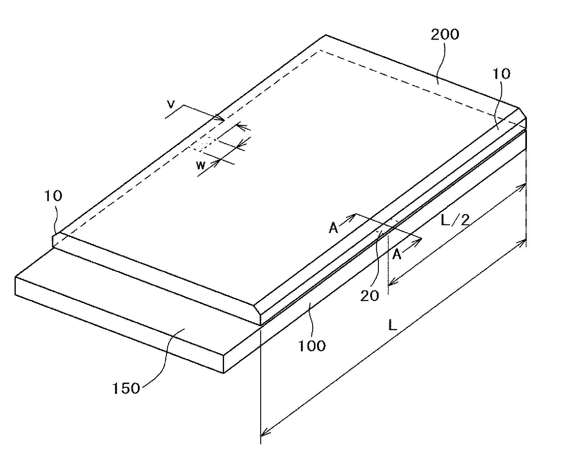
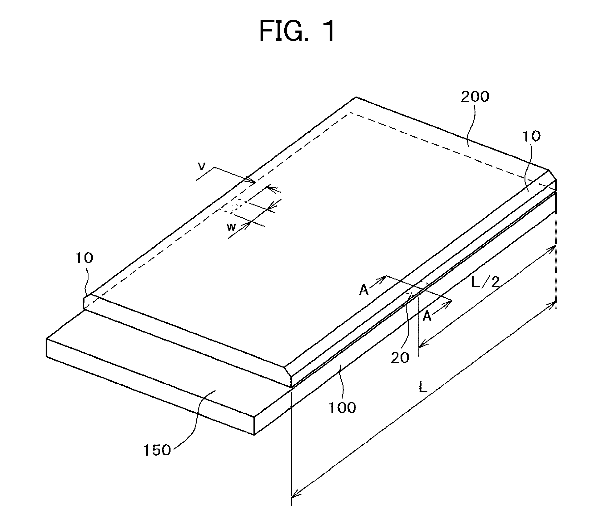
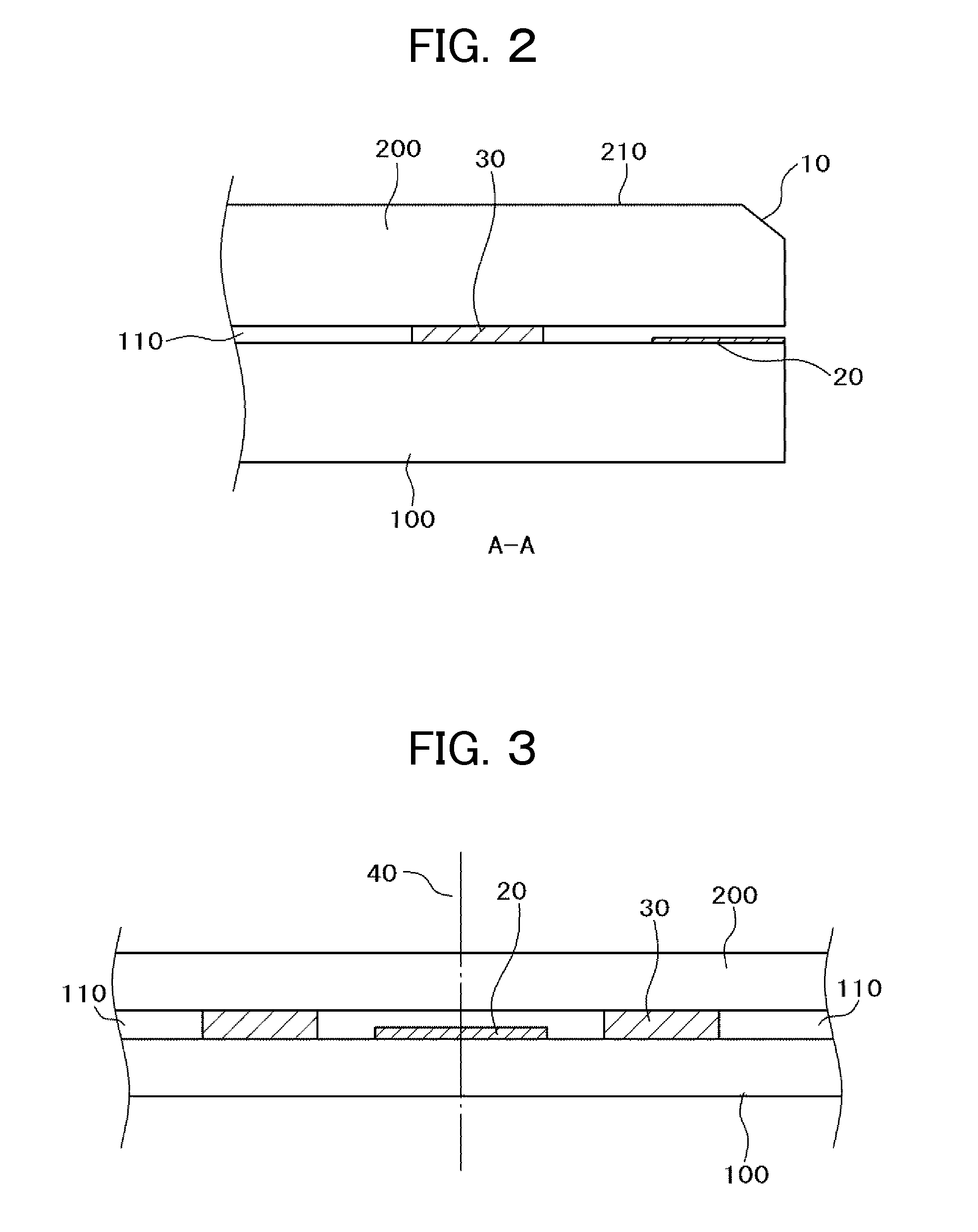
[0030]FIG. 1 is a perspective view of a liquid crystal display device according to the present invention. Both terms “liquid crystal display panel” and “liquid crystal display device” may be used herein, which are interchangeable. Such a liquid crystal display panel can be used, for example, in a mobile phone and the like. In FIG. 1, an opposing substrate 200 formed with a color filter corresponding to each pixel is arranged in an opposing manner on a TFT substrate 100 on which pixels having a TFT and a pixel electrode are arranged in a matrix form. The TFT substrate 100 and the opposing substrate 200 are bonded together by a peripheral sealing material, and liquid crystal is sandwiched by the TFT substrate 100 and the opposing substrate 200. The TFT substrate 100 is formed to be larger than the opposing substrate 200, and a portion consisting of the TFT substrate 100 alone is made to be a terminal portion 150.

[0031]In FIG. 1, two long sides of the opposing substrate 200 are chamfer...


PUM

PropertyMeasurementUnit
sizeaaaaaaaaaa
sizeaaaaaaaaaa
sizeaaaaaaaaaa

Abstract

A liquid crystal display device sandwiching liquid crystal between a TFT substrate having a rectangular plane and an opposing substrate having a rectangular plane, wherein a long side of the TFT substrate is longer than a long side of the opposing substrate, the long side of the opposing substrate is formed with a chamfer, and a light shielding film made of metal is formed on the TFT substrate around a position corresponding to the center of the long side of the opposing substrate. By using the light shielding film, the chipping condition of the opposing substrate near the chamfer can be accurately and rapidly evaluated.

Description

CLAIM OF PRIORITY[0001]The present application claims priority from Japanese Patent Application JP 2012-091466 filed on Apr. 13, 2012, the content of which is hereby incorporated by reference into this application.FIELD OF THE INVENTION[0002]The present invention relates to a display device, and specifically to a liquid crystal display device with an improved bending strength of a liquid crystal display panel.BACKGROUND OF THE INVENTION[0003]A liquid crystal display device is provided with a TFT substrate including a pixel electrode and a thin film transistor (TFT) in a matrix form and an opposing substrate opposing the TFT substrate and formed thereon with a color filter or the like in a position corresponding to the pixel electrode of the TFT substrate, and liquid crystal is sandwiched between the TFT substrate and the opposing substrate. The device forms an image by controlling a light transmission of a liquid crystal molecule with respect to each pixel.[0004]For such a liquid cr...

Claims


Application Information

Patent Timeline
Patent Type & Authority Patents(United States)
IPC IPC(8): G02F1/1335G02F1/1333
CPCG02F1/133512G02F1/133351G02F2001/133388G02F1/133388G02F1/133514G02F1/1368G02F1/136209G02F1/1339
Inventor TATEMURA, MAKOTONAKAMURA, YUICHIITAKURA, MASAHARUOGISHIMA, YOSHITOMO
Owner JAPAN DISPLAY INC
Why Eureka
Try Eureka