Optically monitoring and controlling nanoscale topography

a technology of nanoscale topography and optoelectronic monitoring, applied in the direction of measurement devices, semiconductor/solid-state device testing/measurement, instruments, etc., can solve the problems of duplicate run time and cost, variation, lack of adaptive process control, measurement often requires sample destruction,

Active Publication Date: 2016-02-09
THE BOARD OF TRUSTEES OF THE UNIV OF ILLINOIS
View PDF6 Cites 2 Cited by
  • Summary
  • Abstract
  • Description
  • Claims
  • Application Information

AI Technical Summary

Problems solved by technology

This iterative approach has obvious drawbacks including the added time and cost of duplicate runs, variation due to system drift, and lack of adaptive process control.
Further, the characterization measurement often requires destruction of the sample.
While the sensitivity of these single point or imaging methods can be a few nanometers; however, the measurements are typically hindered by vibrations and drift in the sample.
Maintaining nanoscale accuracy in noisy environments is particularly difficult and represents the main challenge in developing real-time monitoring of dynamic fabrication processes such as wet etching.

Method used


Image

  • Optically monitoring and controlling nanoscale topography
  • Optically monitoring and controlling nanoscale topography
  • Optically monitoring and controlling nanoscale topography

Examples


example i

Unprocessed Wafer

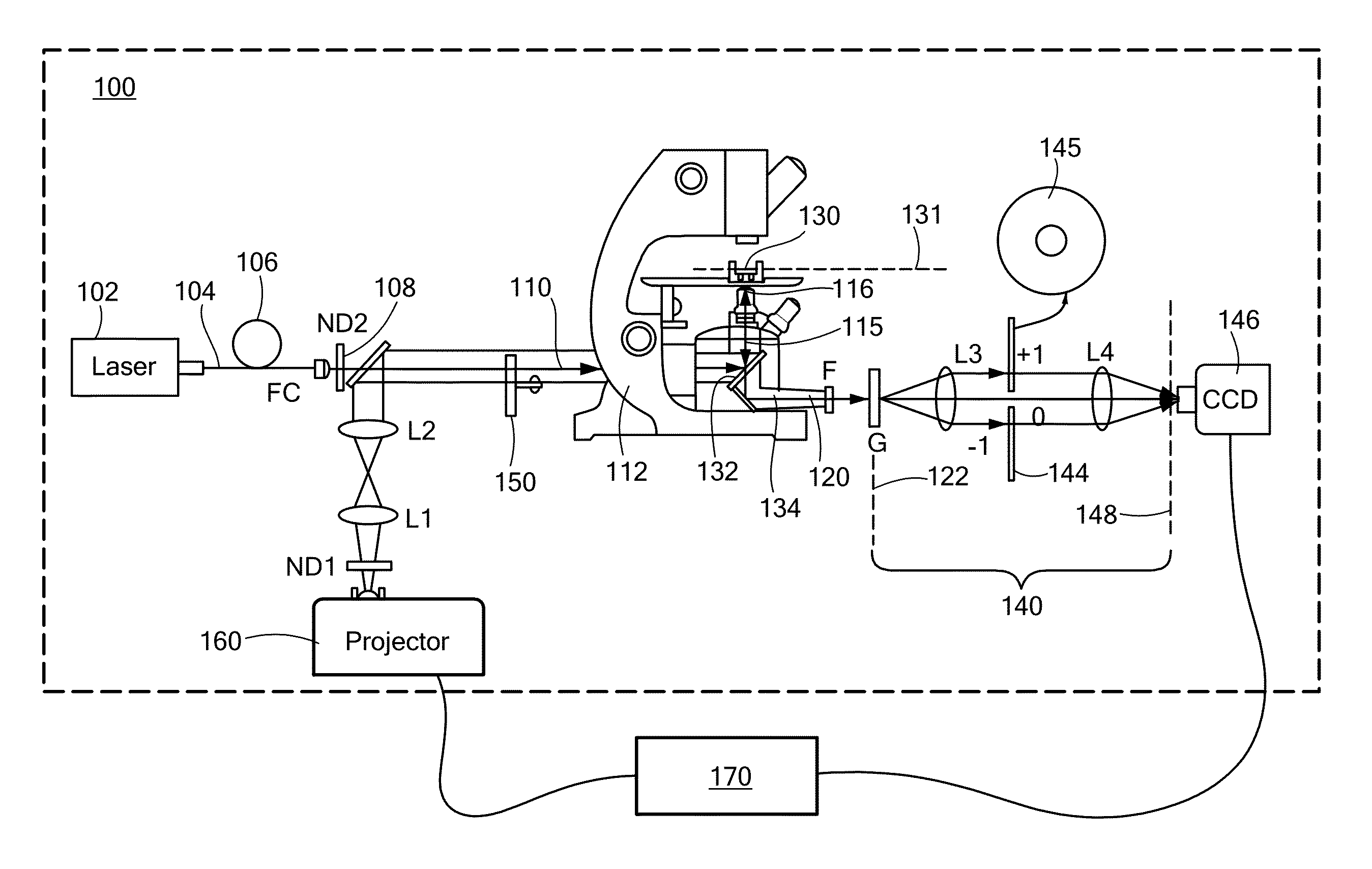
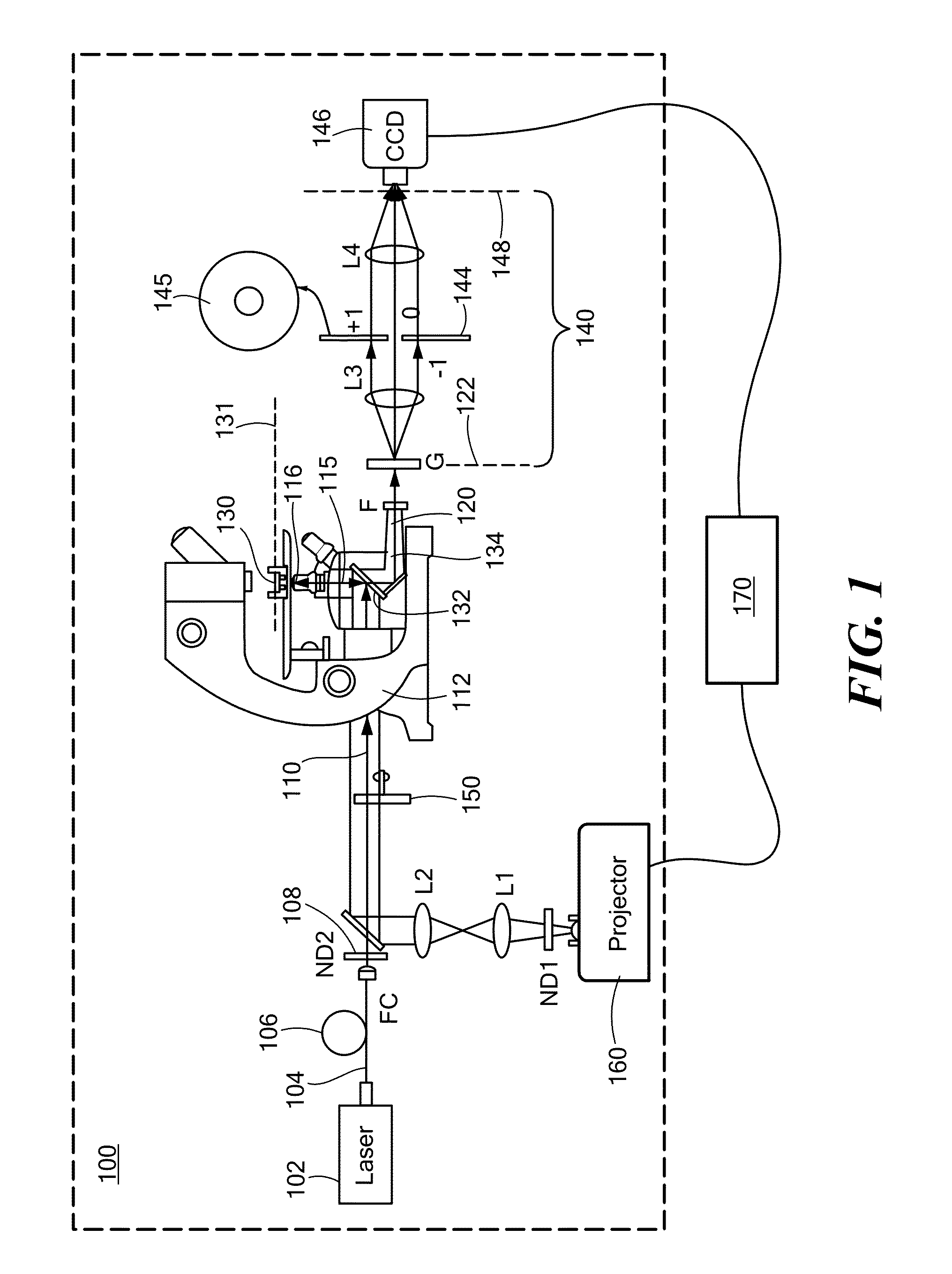
[0045]In accordance with embodiments of the present invention, epi-DPM may provide accurate topographic height maps relative to other points in the image and therefore may be advantageously made insensitive to any common mode motion of the sample. To characterize the spatial and temporal path length noise of the epi-DPM method described herein, a plain, unprocessed n+ GaAs wafer (heavily n-doped) was imaged repeatedly in succession. The successive imaging yielded a time-lapse series of images containing 256 frames at 8.93 frames / s. A 10× objective (NA=0.25) provided a lateral resolution of 1 μm, with a field of view of approximately 160 μm×120 μm. After recovering the height images, a quadratic fit of each individual image was subtracted off. The linear portion of the fit corrects for the tilt of the sample and the angle of interference in camera plane 148 while the quadratic portion corrects for the quadratic phase front of the beam across the field of view. After ...

example ii

Etched Micropillars

[0047]In order to characterize the accuracy of epi-DPM, images of micro-pillars fabricated by wet etching of an n+ GaAs wafer were collected. Photolithography and developing were done using a standard SPR 511A photoresist recipe. A small degree of non-uniformity among multiple micro-pillar heights was observed, which is typical of the fabrication process. For epi-DPM, the spatial standard deviation in height was 6.3 nm for the unetched circular pillar and 4.8 nm for the etched region. The calibration procedure used previously (in Example I) on the flat sample helps but is not as effective on non-planar surfaces.

[0048]FIG. 3A shows the epi-DPM image of a micro-pillar with the diffuser. The positions of the pillar and etched region were extracted from the histogram of the epi-DPM image, as shown in FIG. 3B, by fitting each histogram peak to a separate Gaussian distribution. Although the spatial noise from an individual pixel is several nanometers, the standard error...

example iii

Dynamic Topographic Changes During Etching

[0050]The sensitivity and accuracy results described above underscore the capability of epi-DPM to monitor dynamic topographic changes at the nanoscale. Exploiting this feature, the topography of an n+ GaAs wafer was monitored while being etched with a solution of H3PO4:H2O2:H2O. A total of 400 frames were acquired at 8.93 frames / s, for a total of 44.8 seconds. The resulting epi-DPM movie revealed that it took approximately 10 seconds for the etchant to diffuse into the field of view and begin etching. The montage in FIG. 4A indicates the spatial inhomogeneity and the time evolution of the etching process. The quantitative information provided by epi-DPM allows a measurement of etch rates in a spatially and temporally resolved manner. FIG. 4B plots etch depth profile at discrete points across the sample.

Photochemical Etching

[0051]In combination with epi-DPM, and in accordance with alternate embodiments of the present invention, photochemical...


PUM


Abstract

Methods and apparatus for method for characterizing a height profile of a scattering surface relative to a fiducial plane. The scattering surface, which may be an interface between distinct solid, liquid, gaseous or plasma phases, is illuminated with substantially spatially coherent light, and light scattered by the scattering surface is collected and dispersed, such as by a grating, into zeroth- and first-order beams. A spatial Fourier transform of the zeroth- and first-order beams is created, and one of the beams is low-pass filtered. The beams are interfered at a focal plane detector to generate an interferogram, which is transformed to retrieve a spatially resolved quantitative phase image and / or an amplitude image of the scattering surface. Imaging may be performed during an etching process, and may be used to adaptively control a photoetching process in a feedback loop.

Description

[0001]This invention was made with government support under Grants CBET 1040462, awarded by the National Science Foundation. The Government has certain rights in the invention.TECHNICAL FIELD[0002]The present invention relates to methods and apparatus for monitoring dynamic processes at interfaces between media of distinct optical properties in real time, and, more particularly, to interferometric methods for monitoring and controlling photochemical etching, or liquid-solid-air interfaces, for example.BACKGROUND ART[0003]In order to produce properly functioning semiconductor devices, tight dimensional control is typically required during nanofabrication. In processes such as growth or etching, control of feature size, especially height, is often performed by carrying out an initial calibration run on a dummy wafer, which includes a post-process measurement to determine the growth or etching rate. After this preliminary calibration, the fabrication is run on the real wafer under the ...

Claims


Application Information

Patent Timeline
Patent Type & Authority Patents(United States)
IPC IPC(8): G01B9/02G01B11/24H01L21/66
CPCG01B11/2441H01L22/12
Inventor POPESCU, GABRIELGODDARD, LYNFORDEDWARDS, CHRISARBABI, AMIR
Owner THE BOARD OF TRUSTEES OF THE UNIV OF ILLINOIS
Why Eureka
Try Eureka