Method and apparatus for controlling wafer uniformity using spatially resolved sensors

a technology of spatial resolution and sensor, applied in the field of semiconductor manufacturing, can solve the problems of affecting the underlying topology, affecting the subsequent processing of the wafer, and affecting the quality of the wafer

Inactive Publication Date: 2004-03-16
ADVANCED MICRO DEVICES INC
View PDF10 Cites 37 Cited by
  • Summary
  • Abstract
  • Description
  • Claims
  • Application Information

AI Technical Summary

Problems solved by technology

Such thickness variations, if sufficiently large, may result in defects in the various die defined on the wafer.
Thickness variation across the wafer also complicates subsequent proce

Method used


Image

  • Method and apparatus for controlling wafer uniformity using spatially resolved sensors
  • Method and apparatus for controlling wafer uniformity using spatially resolved sensors
  • Method and apparatus for controlling wafer uniformity using spatially resolved sensors

Examples


Embodiment Construction

Illustrative embodiments of the invention are described below. In the interest of clarity, not all features of an actual implementation are described in this specification. It will of course be appreciated that in the development of any such actual embodiment, numerous implementation-specific decisions must be made to achieve the developers' specific goals, such as compliance with system-related and business-related constraints, which will vary from one implementation to another. Moreover, it will be appreciated that such a development effort might be complex and time-consuming, but would nevertheless be a routine undertaking for those of ordinary skill in the art having the benefit of this disclosure.

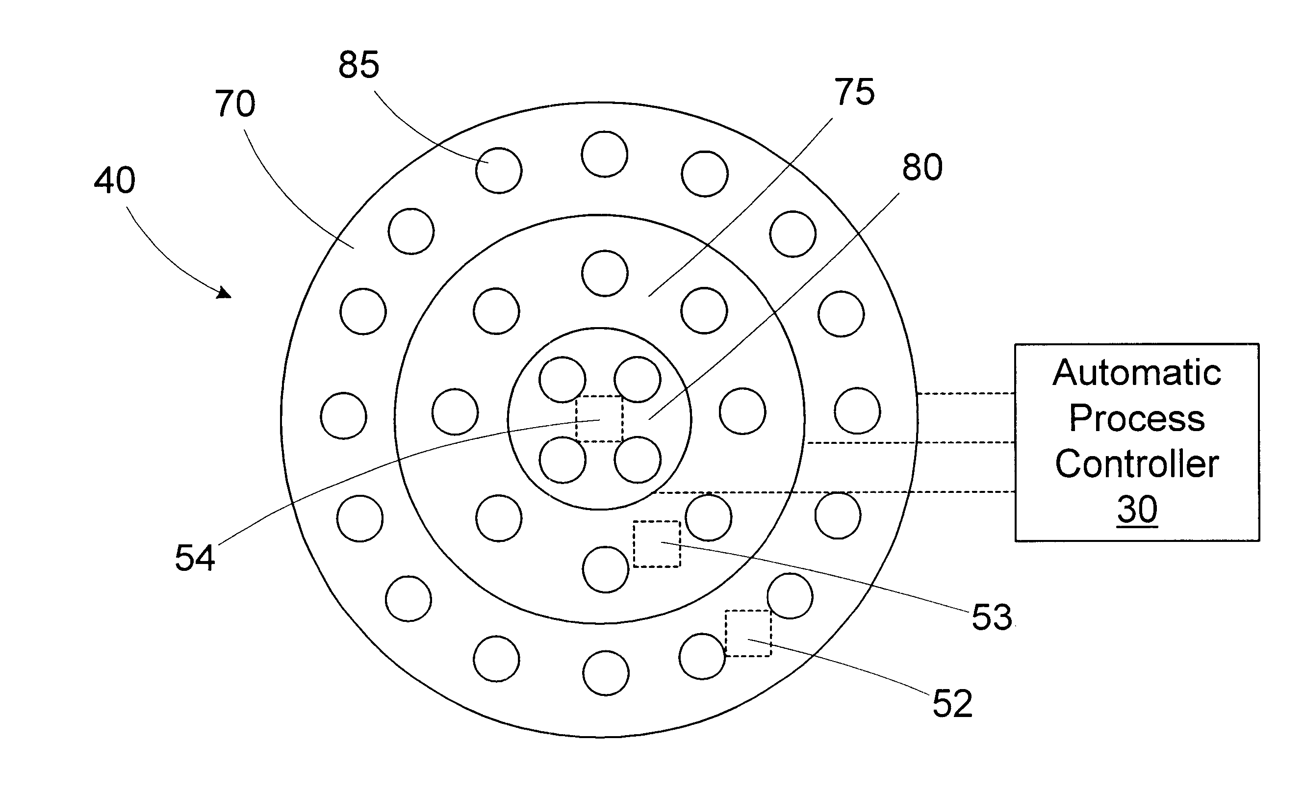
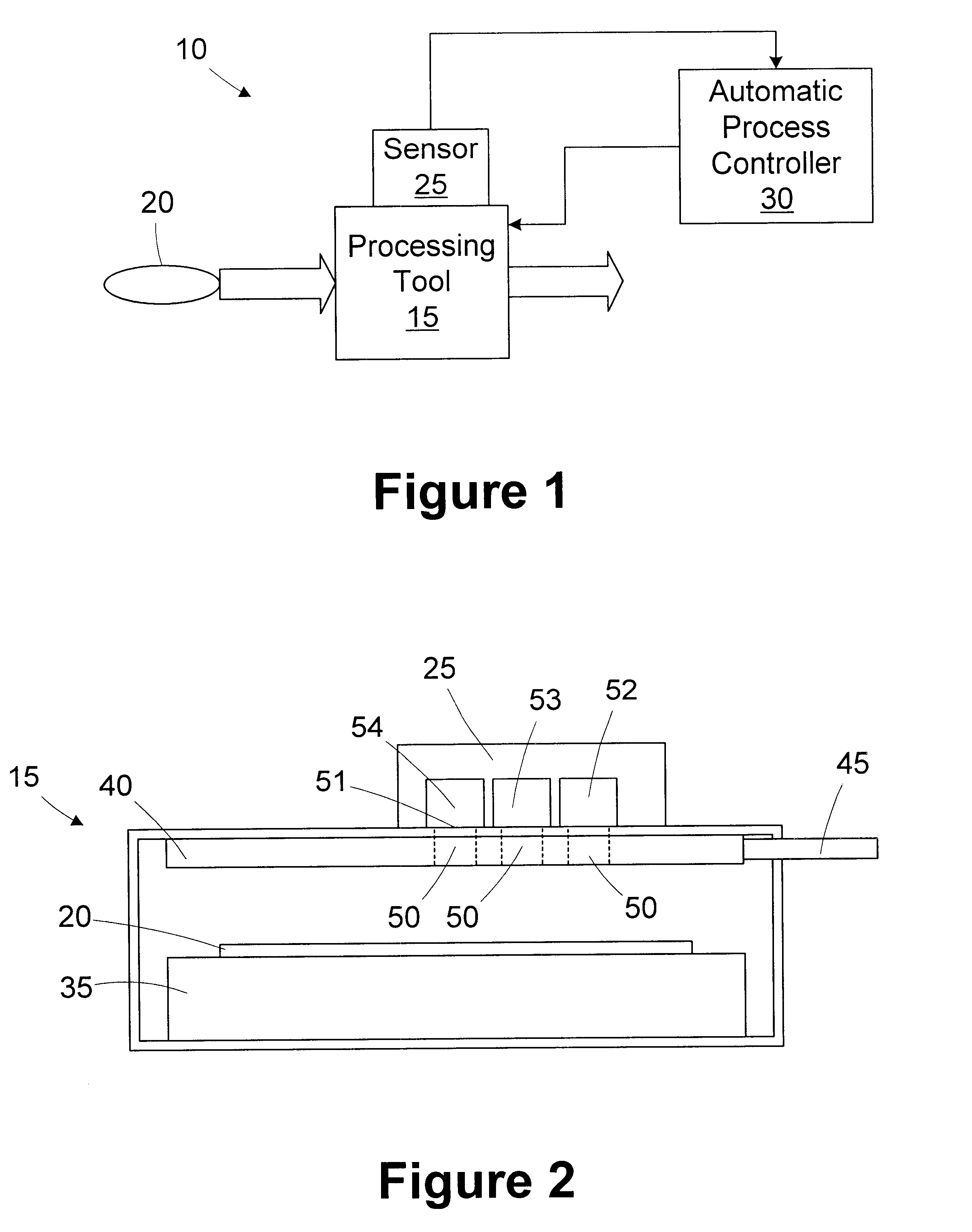
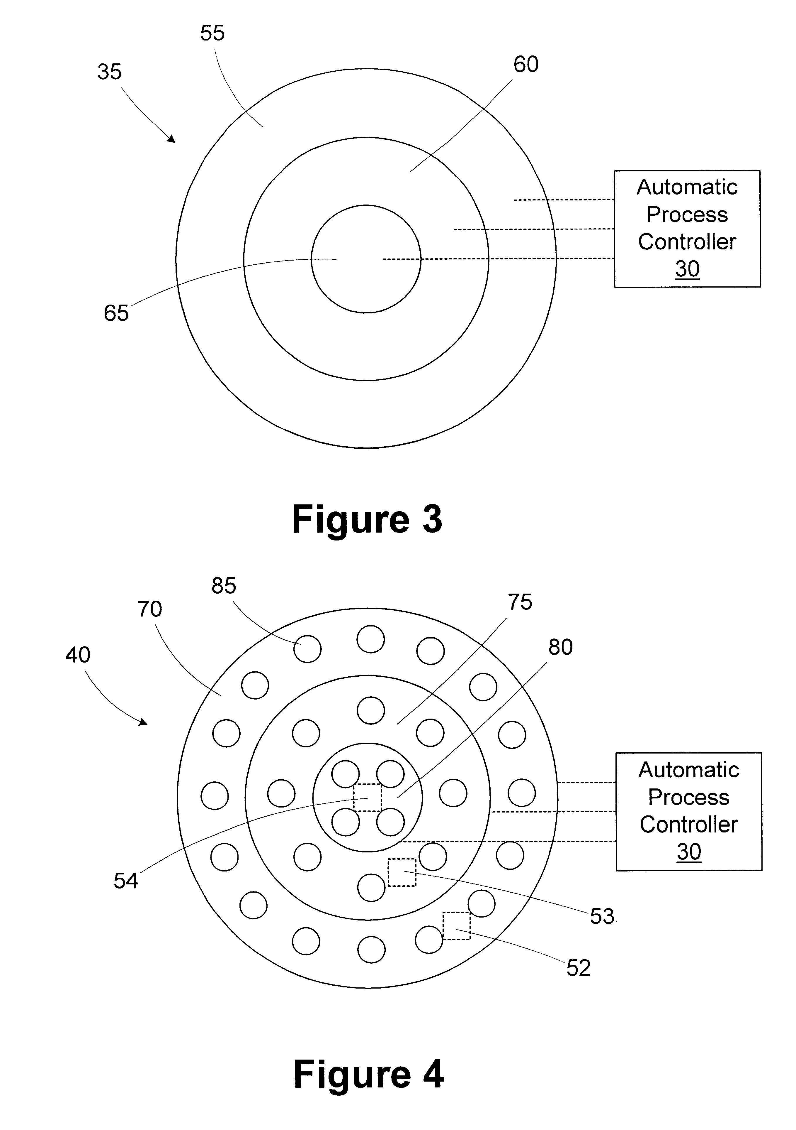
Referring now to the Figures, and in particular, to FIG. 1, a simplified block diagram of a processing system 10 is provided. The processing system 10 includes a processing tool 15 adapted to receive a wafer 20 (i.e., or a lot of wafers 20) and perform at least one processing task on t...


PUM

PropertyMeasurementUnit
Temperatureaaaaaaaaaa
Thicknessaaaaaaaaaa
Poweraaaaaaaaaa

Abstract

A processing system includes a sensor, a processing tool, and an automatic process controller. The sensor has a plurality of sensing regions. The processing tool is adapted to process at least one process layer on a wafer. The process tool includes a process control device controllable by a process control variable. The sensor is adapted to measure a process layer characteristic of the process layer in a selected one of the sensing regions. The automatic process controller is adapted to receive the process layer characteristics measured by the sensor and adjust the process control variable in response to the process layer characteristic measured in one sensing region differing from the process layer characteristic measured in another sensing region. A method for controlling wafer uniformity includes processing a process layer on a wafer; measuring a characteristic of the layer in a plurality of sensing locations; and changing a process control variable of a process control device in response to the process layer characteristic measured in one sensing location differing from the process layer characteristic measured in another sensing location to affect the rate of processing the process layer in at least one of the sensing locations.

Description

1. Field of the InventionThis invention relates generally to semiconductor manufacture, and more particularly, to a method and apparatus for controlling wafer uniformity using spatially resolved sensors.2. Description of the Related ArtIn the manufacture of semiconductor devices, wafers, such as silicon wafers, are subjected to a number of processing steps. The processing steps include depositing or forming layers, patterning the layers, and removing portions of the layers to define features on the wafer. One such process step is the formation of a layer by chemical vapor deposition, where reactive gases are introduced into a vessel containing the semiconductor wafers. The reactive gases facilitate a chemical reaction that causes a layer to form on the wafers.Commonly, variation in the thickness of the deposited layer exists across the wafer. For example, the thickness of the layer deposited on the periphery may be greater or less than the thickness of the layer deposited in the cen...

Claims


Application Information

Patent Timeline
IPC IPC(8): H01J37/32G01B11/06C23C16/52H01L21/66
CPCH01J37/32935H01J37/3299H01L21/00
Inventor TOPRAC, ANTHONY J.MILLER, MICHAEL L.
Owner ADVANCED MICRO DEVICES INC
Why Eureka
Try Eureka