Holding by a memory controller multiple central processing unit memory access requests, and performing the multiple central processing unit memory requests in one transfer cycle

a memory controller and central processing unit technology, applied in the field of memory access control, can solve the problems of reducing the performance of the cpu, reducing the power consumption and cost, etc., and reducing the overhead of data transfer. , the effect of minimizing the access delay

Active Publication Date: 2016-02-23
INT BUSINESS MASCH CORP
View PDF22 Cites 0 Cited by
  • Summary
  • Abstract
  • Description
  • Claims
  • Application Information

AI Technical Summary

Benefits of technology

[0050]As described above, according to the present invention, in a memory system shared by main memory for multiple CPUs and other memories such as a data buffer, when main memory access requests come, memory transfer is enabled while minimizing the access delay and reducing the overhead of the data transfer.

Problems solved by technology

Reduction in power consumption and cost reduction is key issue for a storage device.
A delay from when an access request to the main memory is issued until completion of the request is a latency time of the CPU.
The longer this latency time, the lower the performance of the CPU.
In this method, if respective data transfers get stuck, this ends up an interruption of a host transfer or reduction in media transfer performance.
However, the physical band of the DRAM memory, which is decided based on the bus width and frequency, is limited.
Further, the turn around time of a main memory access affects the performance of the CPU.
Thus, when a memory is shared between the main memory and another DRAM memory, the following problems arise.
However, widening the bus width to increase the bandwidth leads to an increase in the number of chips used, and this defeats the intended purpose of reducing the number of memory parts.
On the other hand, raising the operating frequency leads to an increase in power consumption, and this is not a perfect solution.
However, in the case of main memory accesses for which the turn around time is a key issue, if memory access is being performed by another block when a main memory request comes, the main memory access needs to wait until completion of the current transfer.
It is a possible option to resolve this issue to interrupt the current transfer and allow the main memory transfer, but this cannot be employed in a system with high performance required because this degrades the other blocks' bandwidth.
However, in the case of a memory shared among CPUs used for different purposes, this method is not effective because the memory is used by dividing the physical area of the memory and hence the addresses are not consecutive.
Thus, the CPU access is not efficient in terms of burst transfer, increasing the overhead.
To this end, since a retransfer cycle is required, then the transfer overhead increases, making it difficult to guarantee the bandwidth of the block.

Method used


Image

  • Holding by a memory controller multiple central processing unit memory access requests, and performing the multiple central processing unit memory requests in one transfer cycle
  • Holding by a memory controller multiple central processing unit memory access requests, and performing the multiple central processing unit memory requests in one transfer cycle
  • Holding by a memory controller multiple central processing unit memory access requests, and performing the multiple central processing unit memory requests in one transfer cycle

Examples


Embodiment Construction

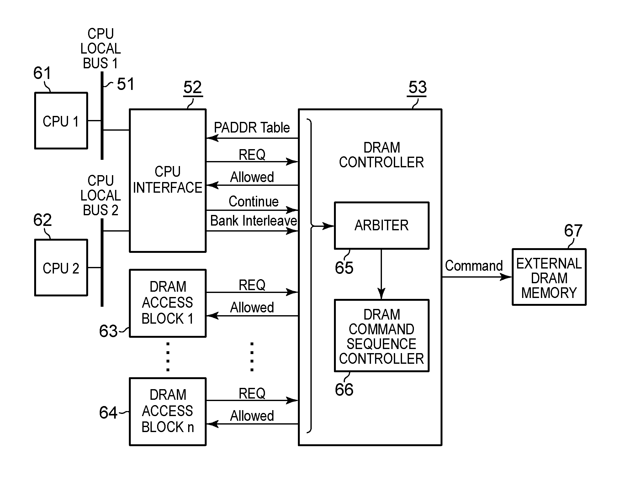
[0058]A DRAM access device according to a preferred embodiment (hereinafter simply called the “embodiment”) of the present invention will be described below in terms of data flows in a recording device and accesses from multiple CPUs. Note that the following embodiment is an illustrative example, and is not intended to limit the content of the present invention.

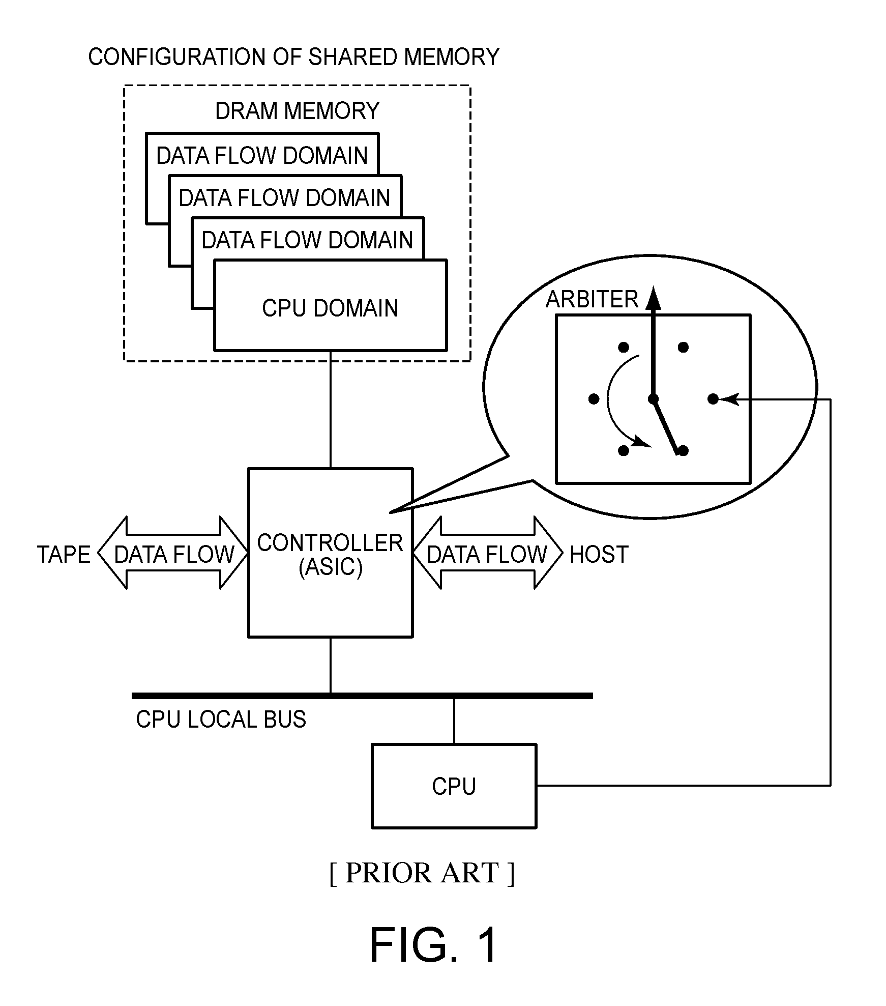
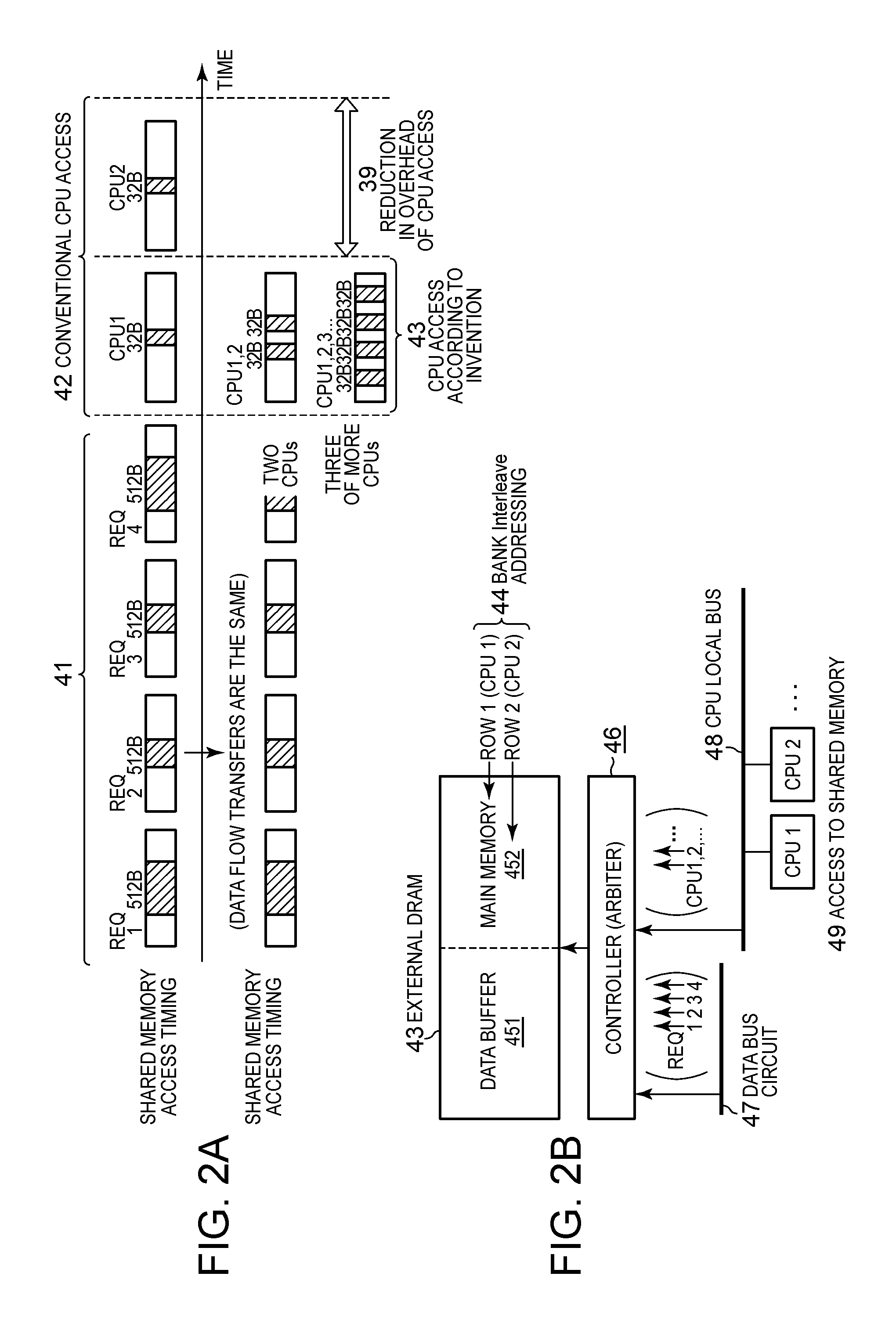
[0059]In a memory system for shared use of main memories for multiple CPUs and another data buffer memory, when a CPU access request comes, the following methods are performed:

[0060](a) When multiple main memory access requests come, if the transfer of another block is being performed, these requests are kept waiting. Then, after completion of the transfer of another block, these two transfer requests are performed in one cycle using a bank interleave (hereinafter also abbreviated as BI) defined in specifications such as DDR3 SDRAM.

[0061](b) When a certain main memory access request comes, if the transfer of another block is ...


PUM


Abstract

The present invention includes a plurality of CPUs using memory as main memory, another function block using memory as a buffer, a CPU interface which controls access transfer from the plurality of CPUs to memory, and a DRAM controller for performing arbitration of the access transfer to the memory. Therein, the CPU interface causes access requests from the plurality of CPUs to wait, and receives and stores the address, data transfer mode and data size of each access, notifies the DRAM controller of the access requests, and then, upon receiving grant signals for the access requests, sends information to the DRAM controller according to the grant signals, whereupon the DRAM controller receives the grant signals, and on the basis of the access arbitration, specifies CPUs for which transfers have been granted so as to send the grant signals to the CPU interface.

Description

FIELD OF THE INVENTION[0001]The present invention relates to memory access control for multiple processors included in an information apparatus.BACKGROUND ART[0002]Reduction in power consumption and cost reduction is key issue for a storage device. For example, reduction in the number of used DRAM memories makes a huge contribution to the reduction in power consumption, cost, and footprint. Recently, SoC LSI equipped with multiple CPUs has been developed. In general, each of the multiple CPUs needs a main memory, respectively. Sharing the multiple CPU memories with other DRAM memories on the LSI can reduce the number of DRAM memories used as the main memories.[0003]FIG. 1 shows an ASIC having a DRAM memory shared between access from a CPU (CPU access) and data flow transfers, and an arbiter enabling the sharing of the memory. In this shared memory configuration, a data buffer for data flows and a main memory of the CPU share the same DRAM memory chip. In the shared memory, usable ar...

Claims


Application Information

Patent Timeline
Patent Type & Authority Patents(United States)
IPC IPC(8): G06F3/00G06F13/16G06F13/00
CPCG06F13/1647G06F13/1642G06F13/1663G06F13/4234G06F13/366G11C7/1048G11C7/1072
Inventor MATSUO, HISATONAGAHARA, RIKAOHTANI, KENJI
Owner INT BUSINESS MASCH CORP
Why Eureka
Try Eureka