Fabrication method of wafer level semiconductor package and fabrication method of wafer level packaging substrate

a fabrication method and semiconductor technology, applied in semiconductor/solid-state device testing/measurement, semiconductor device details, semiconductor/solid-state device testing/measurement, etc., can solve the problems of high fabrication cost, adverse effect of positioning accuracy of semiconductor components, and yield loss in rdl and bump processes, so as to facilitate accurate control of the position of semiconductor components, prevent the position accuracy of semiconductor components from being affected, and increase the position error of semiconductor components

Active Publication Date: 2016-02-23
SILICONWARE PRECISION IND CO LTD
View PDF12 Cites 3 Cited by
  • Summary
  • Abstract
  • Description
  • Claims
  • Application Information

AI Technical Summary

Benefits of technology

[0032]Therefore, the present invention forms the circuit layer before removing the carrier so as to avoid performing an RDL process after removing the carrier, thus preventing the positioning accuracy of semiconductor components from being adversely affected by the CTE and flexibility of a thermal release tape as in the prior art. Therefore, an increase in the size of the carrier does not result in an increase in the position error of the semiconductor components, thereby facilitating accurate control of the position of the semiconductor components.
[0033]Further, the present invention can detect the yield rate of the circuit layer before mounting semiconductor components. If the circuit layer is detected to be of low quality, the structure is directly discarded without performing subsequent processes such as mounting semiconductor components. Therefore, the present invention does not discard good semiconductor components as in the prior art when the circuit layer is detected to be of low quality, thereby saving material costs and achieving cost efficiency.

Problems solved by technology

However, since the thermal release tape 11 is flexible, the positioning accuracy of the semiconductor components 12 is adversely affected by the CTE (Coefficient of Thermal Expansion) of the thermal release tape 11 and lateral forces applied on the thermal release tape 11 by the encapsulant 13 during the molding process.
Therefore, an increase in the size of carrier 10 results in an increase in the position error of the semiconductor components 12, thereby causing yield losses in the RDL and bump processes.
That is, good semiconductor components 12 are also discarded, thus resulting in a high fabrication cost.
Therefore, the above-described method is not economic.

Method used


Image

  • Fabrication method of wafer level semiconductor package and fabrication method of wafer level packaging substrate
  • Fabrication method of wafer level semiconductor package and fabrication method of wafer level packaging substrate
  • Fabrication method of wafer level semiconductor package and fabrication method of wafer level packaging substrate

Examples


Embodiment Construction

[0037]The following illustrative embodiments are provided to illustrate the disclosure of the present invention, these and other advantages and effects can be apparent to those in the art after reading this specification.

[0038]It should be noted that the drawings are only for illustrative purposes and not intended to limit the present invention. Meanwhile, terms such as ‘on’, ‘a’ etc. are only used as a matter of descriptive convenience and not intended to have any other significance or provide limitations for the present invention.

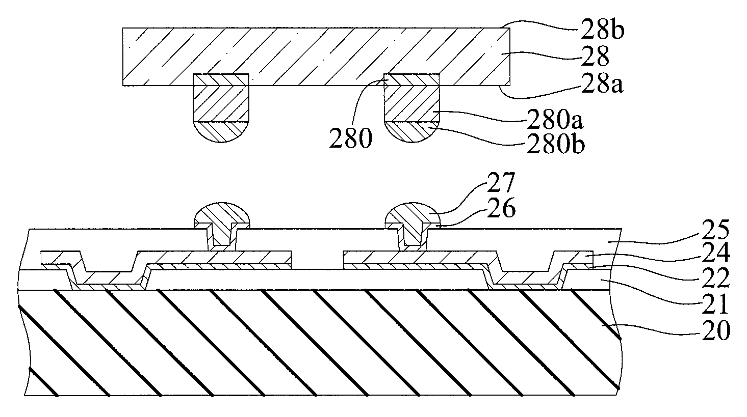
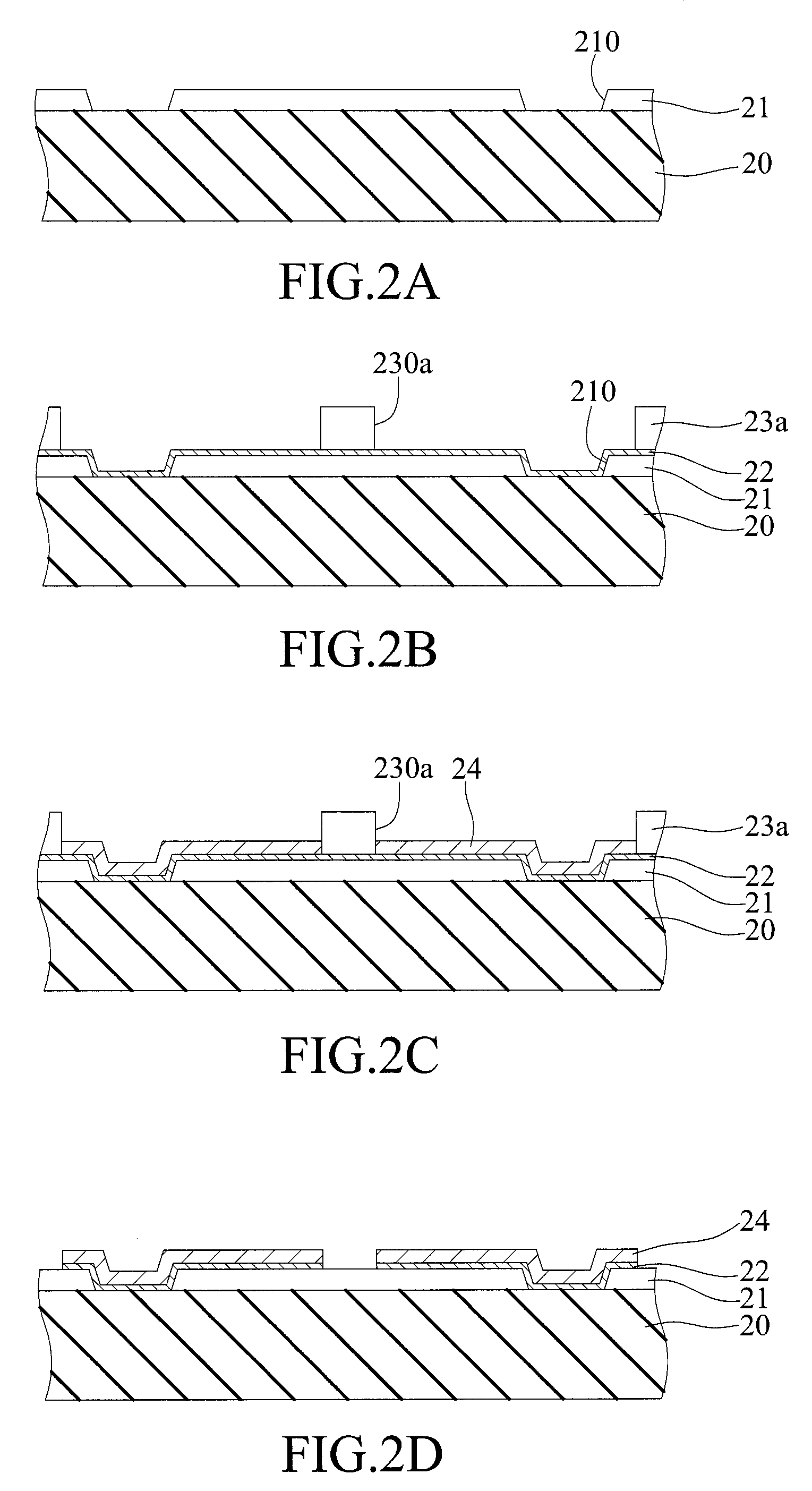
[0039]FIGS. 2A to 2K are schematic cross-sectional views showing a fabrication method of a wafer level semiconductor package 2 according to the present invention.

[0040]Referring to FIG. 2A, a first dielectric layer 21 is formed on a carrier 20 by coating, and further patterned such that a plurality of openings 210 are formed in the first dielectric layer 21 for exposing portions of the carrier 20.

[0041]In the present embodiment, the first dielectric layer...


PUM


Abstract

A fabrication method of a wafer level semiconductor package includes: forming on a carrier a first dielectric layer having first openings exposing portions of the carrier; forming a circuit layer on the first dielectric layer, a portion of the circuit layer being formed in the first openings; forming on the first dielectric layer and the circuit layer a second dielectric layer having second openings exposing portions of the circuit layer; forming conductive bumps in the second openings; mounting a semiconductor component on the conductive bumps; forming an encapsulant for encapsulating the semiconductor component; and removing the carrier to expose the circuit layer. By detecting the yield rate of the circuit layer before mounting the semiconductor component, the invention avoids discarding good semiconductor components together with packages as occurs in the prior art, thereby saving the fabrication cost and improving the product yield.

Description

CROSS-REFERENCES TO RELATED APPLICATIONS[0001]This application claims under 35 U.S.C. §119(a) the benefit of Taiwanese Application No. 101109611, filed Mar. 21, 2012, the entire contents of which is incorporated herein by reference.BACKGROUND OF THE INVENTION[0002]1. Field of the Invention[0003]The present invention relates to fabrication methods of semiconductor packages, and more particularly, to a fabrication method of a wafer level semiconductor package and a fabrication method of a wafer level packaging substrate for improving the product accuracy.[0004]2. Description of Related Art[0005]Along with the rapid development of electronic industries, electronic products are developed towards multi-function and high performance. To meet the miniaturization requirement of semiconductor packages, wafer level packaging (WLP) technologies have been developed.[0006]U.S. Pat. No. 6,452,265 and U.S. Pat. No. 7,202,107 provide fabrication methods of wafer-level packages. FIGS. 1A to 1E are s...

Claims


Application Information

Patent Timeline
Patent Type & Authority Patents(United States)
IPC IPC(8): H01L21/00H01L21/683H01L21/48H01L23/31H01L23/498H01L21/56H01L23/00H01L21/66H01L25/065
CPCH01L21/6835H01L21/4857H01L23/49822H01L24/97H01L21/563H01L21/568H01L22/14H01L22/20H01L23/3128H01L23/3185H01L23/49816H01L24/11H01L24/13H01L24/16H01L24/81H01L25/0657H01L2221/68345H01L2221/68359H01L2221/68381H01L2224/11849H01L2224/131H01L2224/133H01L2224/1319H01L2224/1329H01L2224/13082H01L2224/16225H01L2224/16227H01L2224/32225H01L2224/73204H01L2224/81005H01L2224/81193H01L2224/81815H01L2224/97H01L2225/06517H01L2924/15311H01L2924/18161H01L2924/00014H01L2924/014H01L2924/00012H01L2924/00H01L2224/81H01L2224/83
Inventor CHEN, LU-YI
Owner SILICONWARE PRECISION IND CO LTD
Why Eureka
Try Eureka