Semiconductor device and operating method thereof

a technology of a semiconductor and an operating method, which is applied in the direction of redundant data error correction, redundant hardware error correction, instruments, etc., can solve the problems of multi-bit error and inability to correct the sensed error

Active Publication Date: 2016-04-05
SK HYNIX INC
View PDF58 Cites 2 Cited by
  • Summary
  • Abstract
  • Description
  • Claims
  • Application Information

AI Technical Summary

Benefits of technology

[0011]Also, various embodiments may be directed to a semiconductor memory device capable of guaranteeing the reliability of data by managing a problem that a single-bit error occurring in a semiconductor memory device develops to a multi-bit error, and an operating method thereof.
[0012]Also, various embodiments may be directed to a semiconductor memory device capable of guaranteeing the reliability of data by relieving a storage space of a semiconductor memory device in which a multi-bit error occurred, using a separate memory device, and an operating method thereof.

Problems solved by technology

However, when a two or more-bit error occurs, the ECC block 12 may sense the error, but cannot correct the sensed error.
The method may further include reporting a multi-bit error when the multi-bit error exists in the data outputted from the first memory device.

Method used


Image

  • Semiconductor device and operating method thereof
  • Semiconductor device and operating method thereof
  • Semiconductor device and operating method thereof

Examples


Embodiment Construction

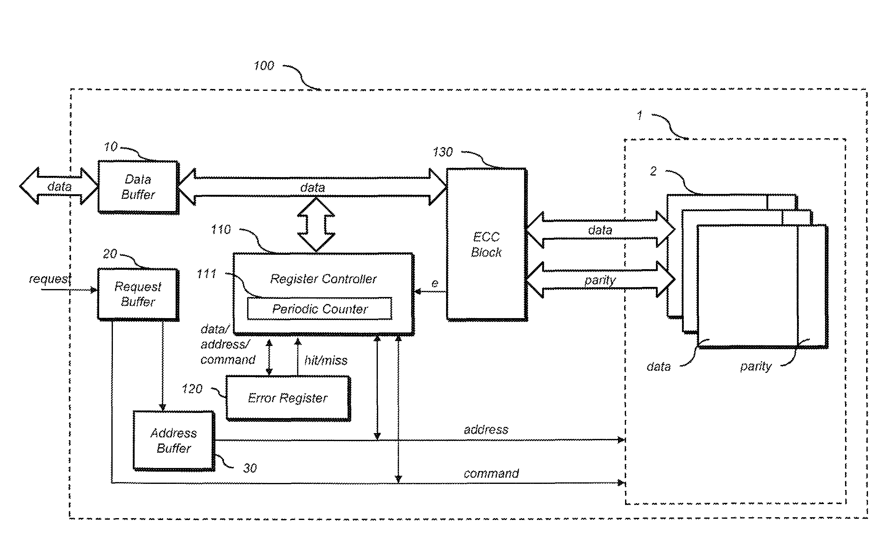
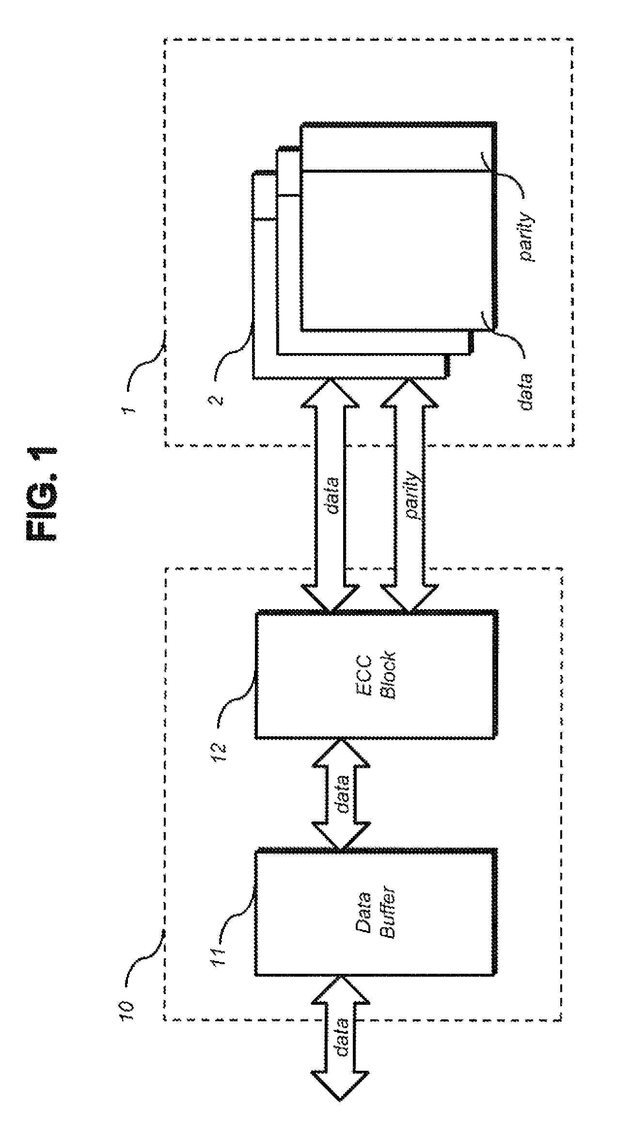
[0049]Various embodiments will be described below in more detail with reference to the accompanying drawings. The present invention may, however, be embodied in different forms and should not be construed as limited to the embodiments set forth herein. Rather, these embodiments are provided so that this disclosure will be thorough and complete, and will fully convey the scope of the present invention to those skilled in the art. Throughout the disclosure, like reference numerals refer to like parts throughout the various figures and embodiments of the present invention.

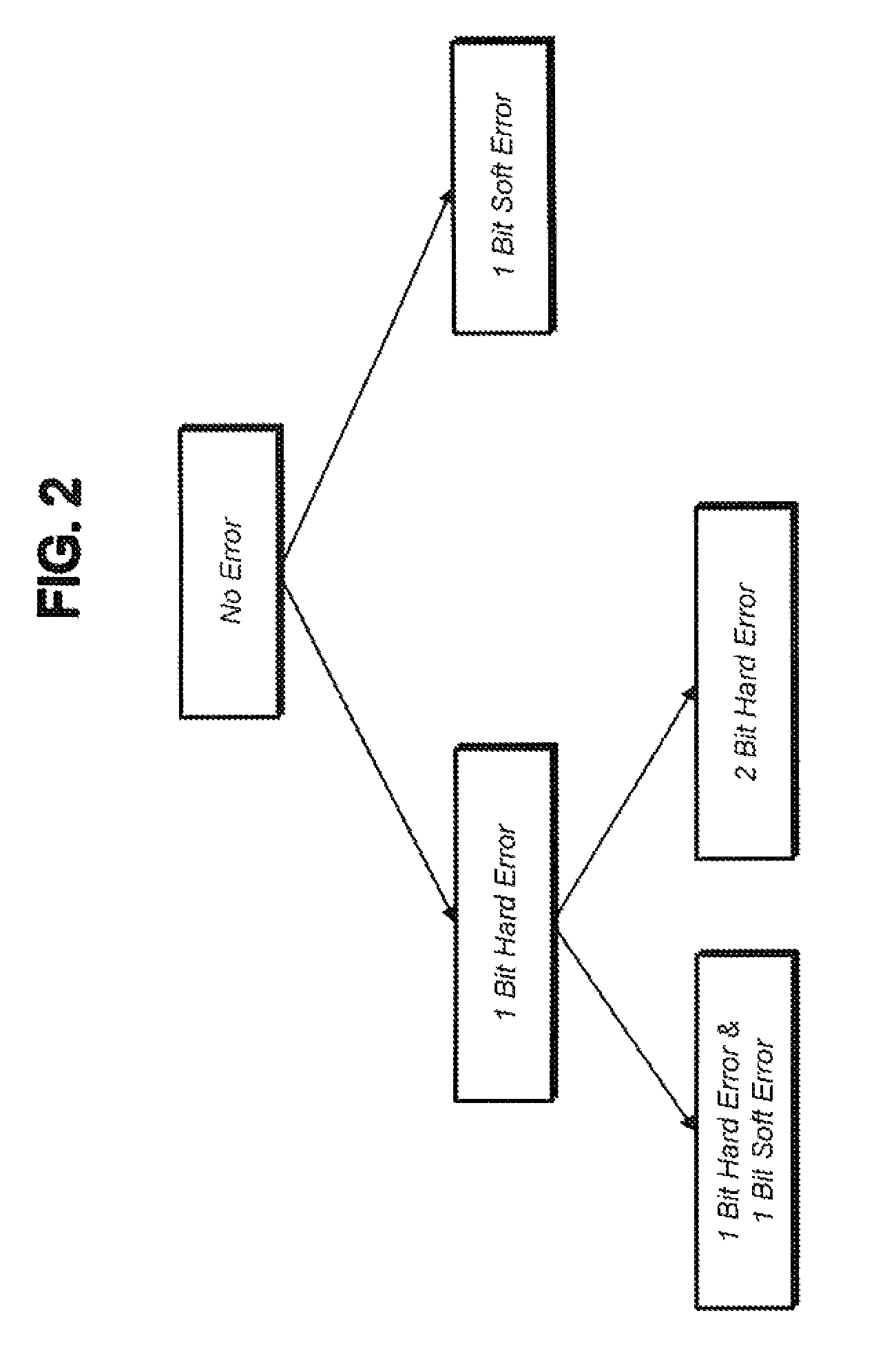
[0050]FIG. 2 is a block diagram illustrating the types of errors managed by a semiconductor device in accordance with an embodiment of the present invention.

[0051]The probability that a multi-bit error will occur at a time at an arbitrary address of a semiconductor memory device is almost close to zero. Therefore, it may safely be said that a multi-bit error may generally develop from a single-bit error.

[0052]A soft e...


PUM


Abstract

A semiconductor device includes a controller configured to receive a request for a first memory device, determine whether or not a multi-bit error has occurred at a requested address of the first memory device, and process the request on a second memory device instead of the first memory device, when the multi-bit error has occurred.

Description

CROSS-REFERENCE TO RELATED APPLICATIONS[0001]The present application claims priority of Korean Patent Application No. 10-2012-0060065, filed on Jun. 4, 2012, which is incorporated herein by reference in its entirety.BACKGROUND[0002]1. Field[0003]Various embodiments of the present invention relate to a semiconductor device and an operating method thereof, and more particularly, to a semiconductor device capable of relieving a multi-bit error and an operating method thereof.[0004]2. Description of the Related Art[0005]FIG. 1 is a block diagram of a conventional semiconductor device 10.[0006]The conventional semiconductor device 10 includes a data buffer 11 configured to transmit and receive data according to an external request and an Error-Correcting Code (ECC) block 12 configured to sense and correct an error of data read from a semiconductor memory device 1.[0007]The ECC block 12 generates parity information corresponding to data when a write request is made, and stores the data an...

Claims


Application Information

Patent Timeline
Patent Type & Authority Patents(United States)
IPC IPC(8): G06F11/10G06F11/20G06F11/14G06F11/16G11C29/04
CPCG06F11/1048G06F11/1024G06F11/141G06F11/1666G06F11/2094G11C2029/0411G11C29/42
Inventor MOON, YOUNG-SUKLEE, HYUNG-DONGKWON, YONG-KEEKIM, HONG-SIKYANG, HYUNG-GYUNKIM, JOON-WOO
Owner SK HYNIX INC
Why Eureka
Try Eureka