

Precursors for silicon dioxide gap fill
a silicon dioxide and gap filling technology, applied in the direction of coatings, semiconductor devices, chemical vapor deposition coatings, etc., can solve the problems of uneven material densification adversely affecting device performance, and becoming progressively more difficult to deposit silicon dioxide in the narrow trenches without introducing, etc., to achieve the effect of suppressing adverse seam effects
- Summary
- Abstract
- Description
- Claims
- Application Information
AI Technical Summary
Benefits of technology
Problems solved by technology
Method used
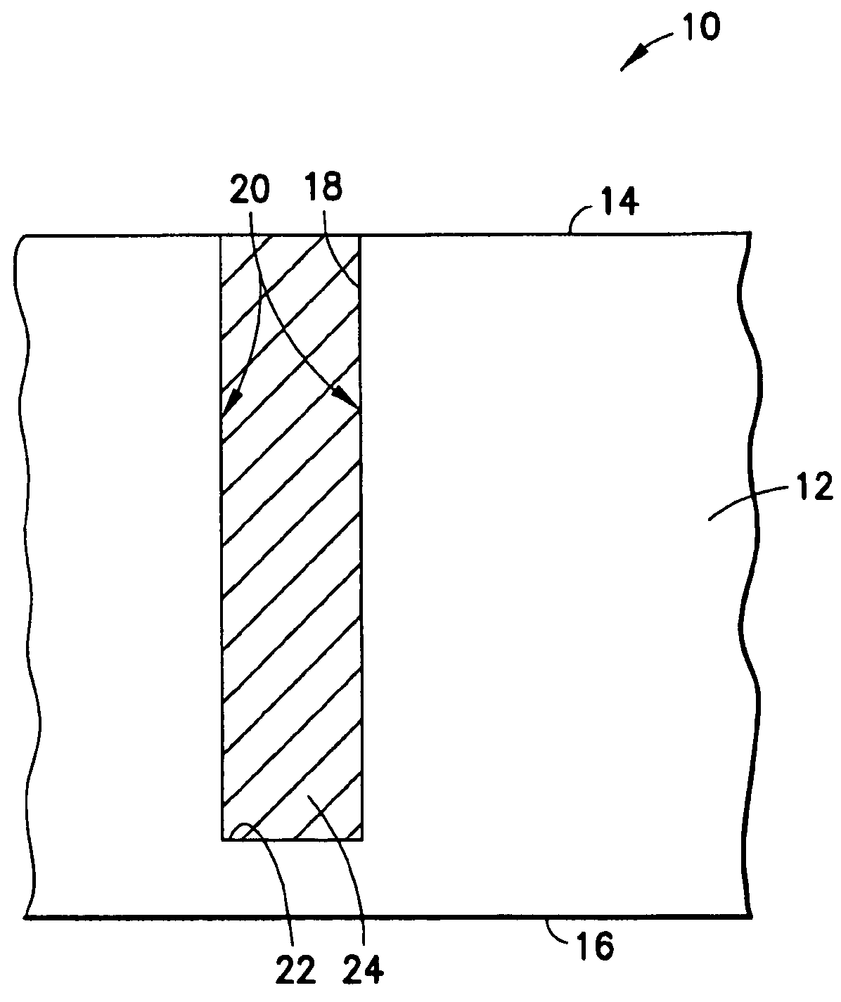
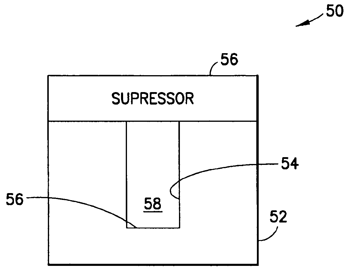
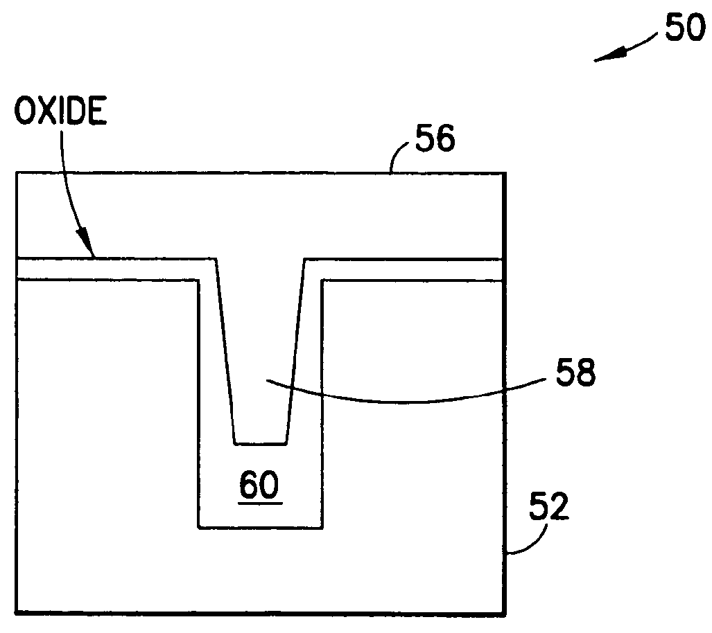
Image

Examples
process examples
Gap Fill Process Examples
[0106]Deposition was carried out in an Applied Materials P5000 reactor with the TEOS / ozone process. Void fraction was found by measuring the void area in SEM cross-sections after cleaving and staining in 200:1 H2O:HF. Stain times were chosen to result in 5 nm removal of SiO2 from blanket film witness pieces deposited in the same run. Results are set out below in the tables for Examples 1, 2 and 3.
example 1
[0107]
ParameterValueTEOS firstStabilize in TEOS 90 seconds beforedepositionPressure500TorrSusceptor Temperature425 CFormulation: IPA / Methanol / TEOS4:4:1Liquid Flow0.433 cc / minOzonator feed gas10SLM O2 + 100 ppm N2Ozone Concentration12%Susceptor spacing420 milsVoid % Annealed (800 C 30 min)10.57Void % As deposited6.88Rate4.5 A / sectime for 2000A444 seconds
example 2
[0108]
ParameterValueTEOS firstStabilize in TEOS 90 seconds beforedepositionPressure500TorrSusceptor Temperature425 CFormulation:IPA:Ethanol:TMOG:TEOS0.05:0.10:0.05:1Liquid Flow0.35 cc / minOzonator feed gas10SLM O2 + 100 ppm N2Ozone Concentration15%Susceptor spacing420 milsGe content (film)2 atomic %Void % Annealed (800 C 30 min)3.59%Void % As deposited1.86Rate10 A / sec
PUM
| Property | Measurement | Unit |
|---|---|---|
| temperature | aaaaa | aaaaa |
| temperature | aaaaa | aaaaa |
| temperature | aaaaa | aaaaa |
Abstract
Description
Claims
Application Information