3D imaging with multiple irradiation frequencies

a technology of 3d imaging and irradiation frequency, applied in the field of semiconductor devices, can solve the problems of affecting the performance of semiconductor devices, and many existing non-destructive analysis tools lack the resolution necessary to accurately obtain measurements of physical features

Active Publication Date: 2016-05-31
ADVANCED MICRO DEVICES INC
View PDF14 Cites 7 Cited by
  • Summary
  • Abstract
  • Description
  • Claims
  • Application Information

AI Technical Summary

Problems solved by technology

During fabrication, process variations may result in semiconductor devices having physical features that deviate from their intended physical dimensions, thereby impairing performance of those devices.
However, many existing non-destructive analysis tools lack the resolution necessary to accurately obtain measurements of physical features, particularly as device geometries continue decreasing in size.

Method used


Image

  • 3D imaging with multiple irradiation frequencies
  • 3D imaging with multiple irradiation frequencies
  • 3D imaging with multiple irradiation frequencies

Examples


Embodiment Construction

[0012]The following detailed description is merely illustrative in nature and is not intended to limit the embodiments of the subject matter or the application and uses of such embodiments. As used herein, the word “exemplary” means “serving as an example, instance, or illustration.” Any implementation described herein as exemplary is not necessarily to be construed as preferred or advantageous over other implementations. Furthermore, there is no intention to be bound by any expressed or implied theory presented in the preceding technical field, background, brief summary or the following detailed description.

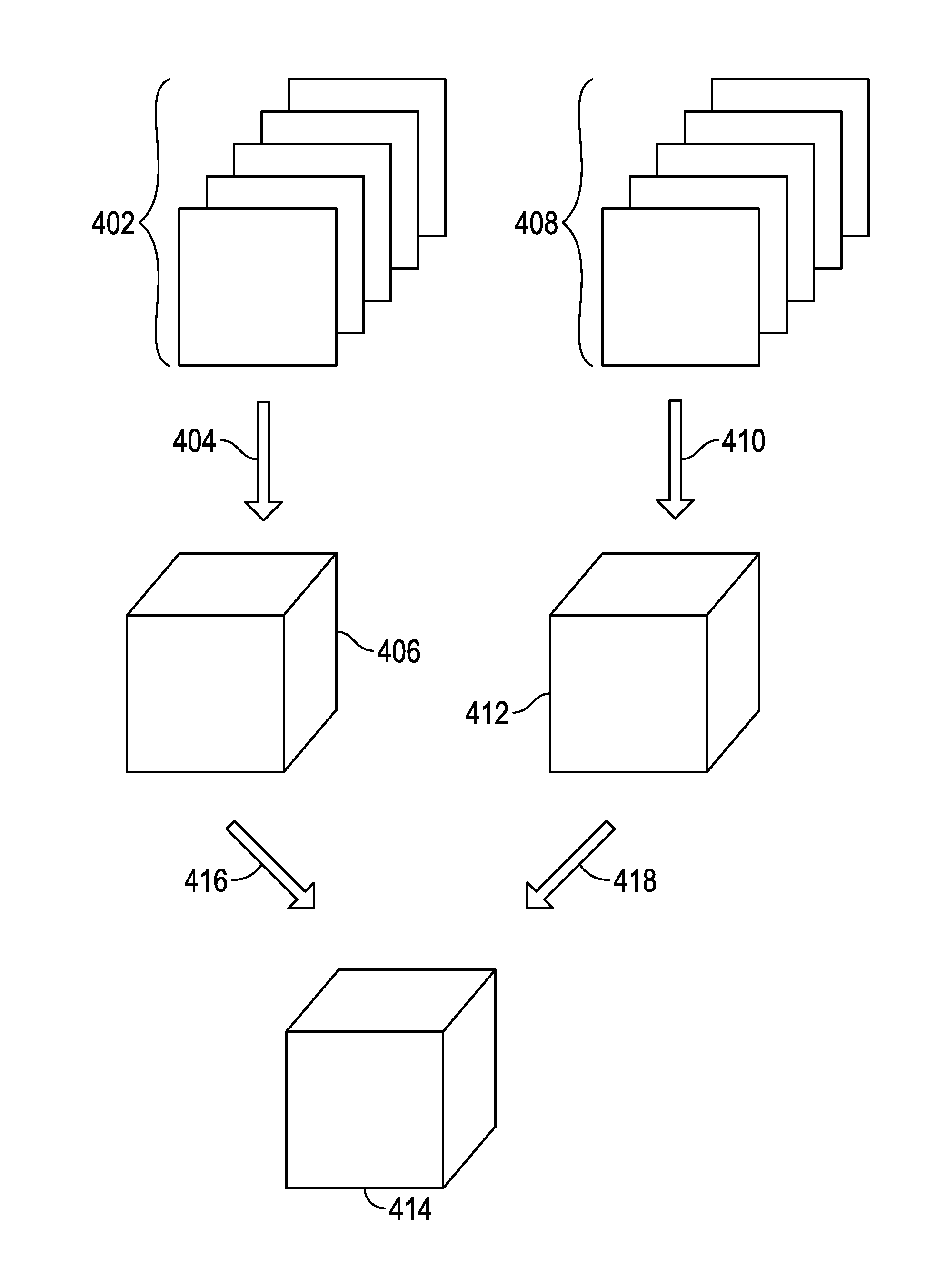
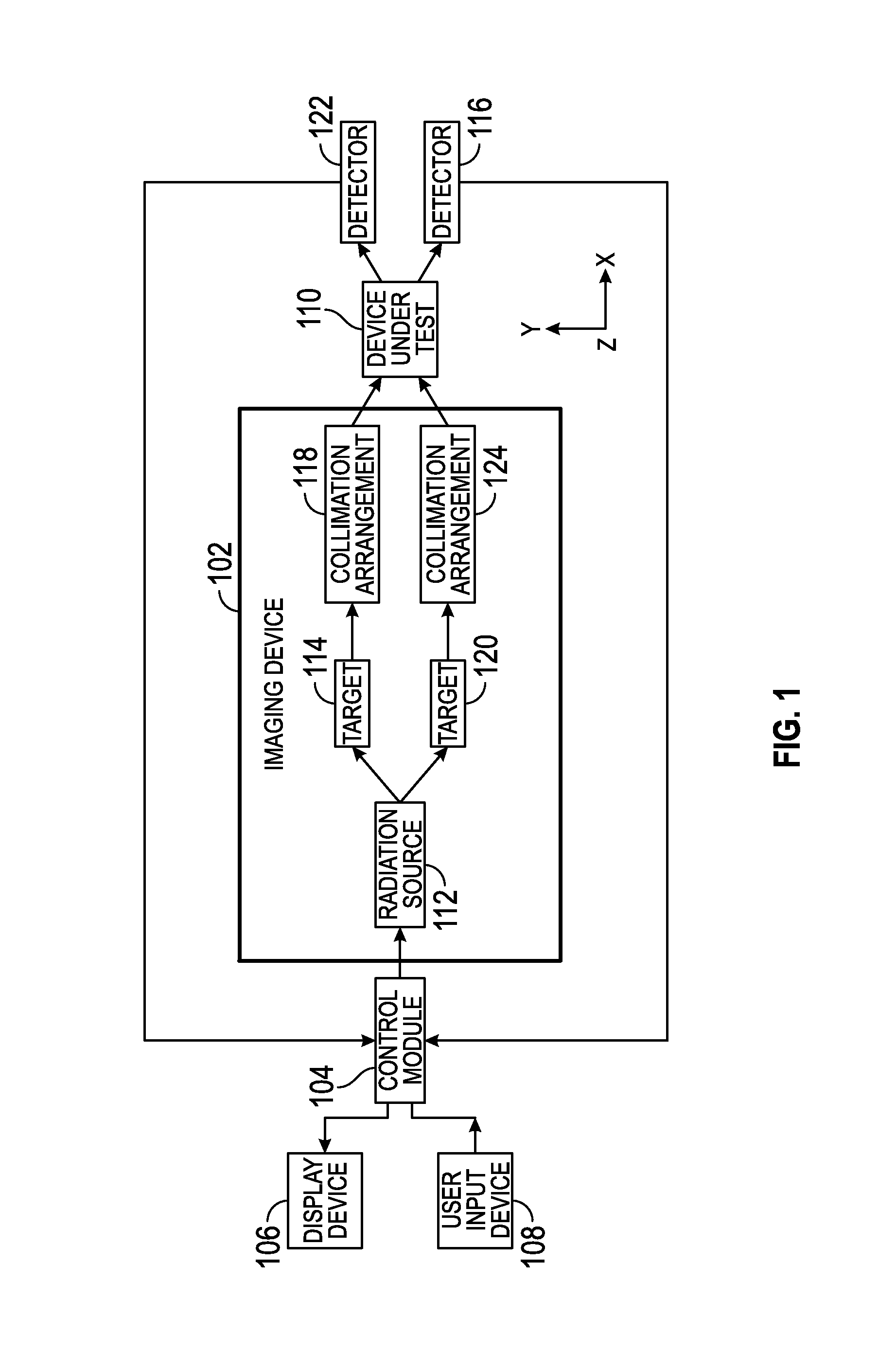
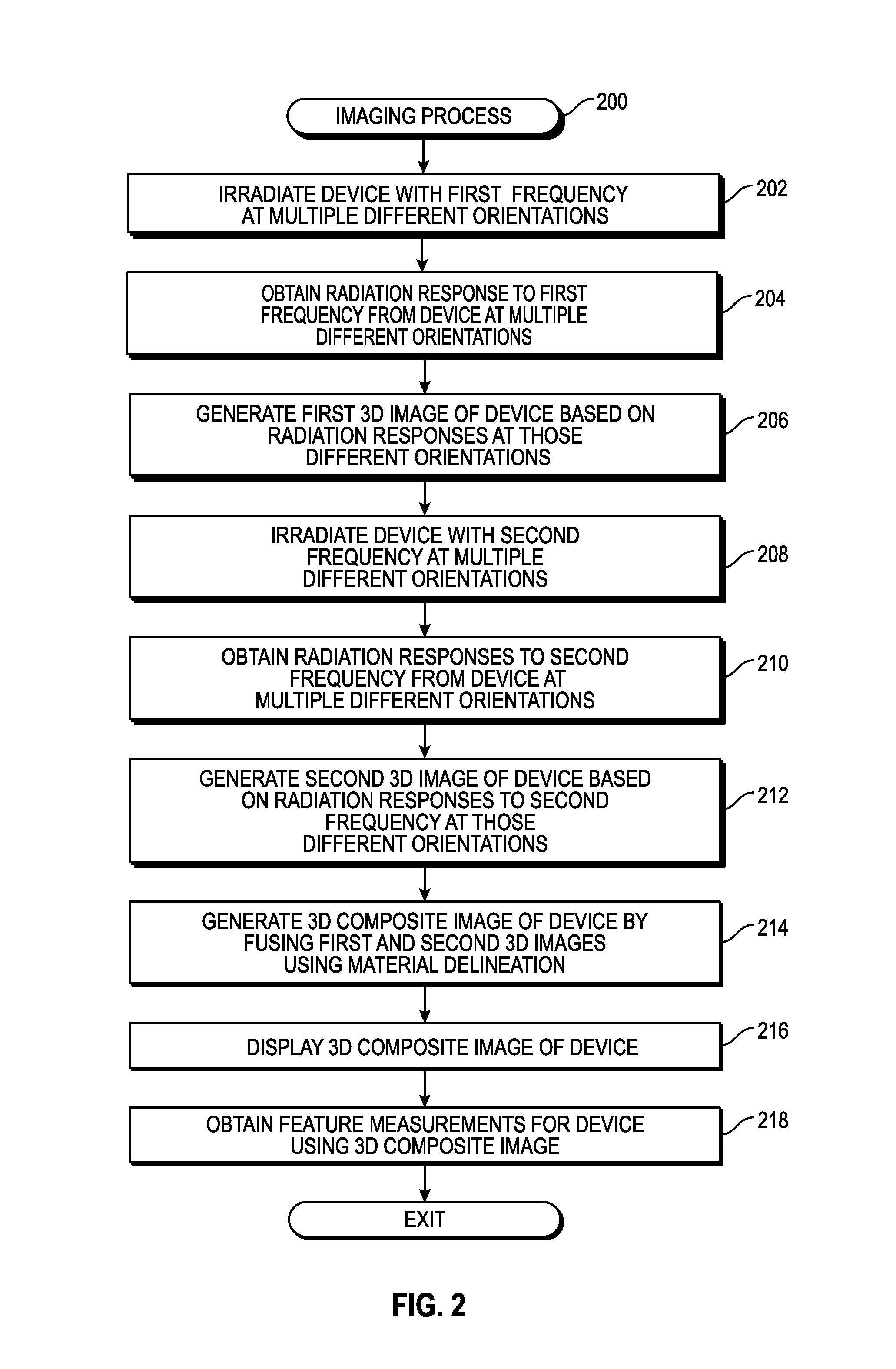
[0013]Embodiments of the subject matter described herein relate to devices, systems, and methods for generating accurate three-dimensional images using multiple different frequencies of electromagnetic radiation for imaging an object, such as a semiconductor device or another device under test. As described in greater detail below, in exemplary embodiments, the object is irradia...


PUM

PropertyMeasurementUnit
anglesaaaaaaaaaa
frequencyaaaaaaaaaa
frequenciesaaaaaaaaaa

Abstract

Imaging methods, apparatus and systems are provided for using different irradiation frequencies to generate a composite three-dimensional image. One exemplary method for imaging a semiconductor device involves irradiating the semiconductor device with a first frequency of electromagnetic radiation, obtaining a first radiation response from the semiconductor device in response to the first frequency of electromagnetic radiation, irradiating the semiconductor device with a second frequency of electromagnetic radiation, obtaining a second radiation response from the semiconductor device in response to the second frequency of electromagnetic radiation, and generating a composite image of the semiconductor device based at least in part on the first radiation response and the second radiation response.

Description

TECHNICAL FIELD[0001]Embodiments of the subject matter described herein relate generally to semiconductor devices, and more particularly, relate to obtaining accurate images of a semiconductor device using different frequencies of electromagnetic radiation.BACKGROUND[0002]Semiconductor devices are used in the vast majority of electronic devices. To ensure devices function in their intended manner, it is desirable to accurately and precisely fabricate physical features having specific physical dimensions. During fabrication, process variations may result in semiconductor devices having physical features that deviate from their intended physical dimensions, thereby impairing performance of those devices. For failure analysis, it is desirable to accurately analyze physical features of a semiconductor device in a non-destructive manner. However, many existing non-destructive analysis tools lack the resolution necessary to accurately obtain measurements of physical features, particularly...

Claims


Application Information

Patent Timeline
Patent Type & Authority Patents(United States)
IPC IPC(8): G01N23/04G01N23/08G01N23/083H01J35/04
CPCG01N23/046G01N23/04G01N23/083H01J35/04G06T2207/30148
Inventor BARAKAT, FARIDBRUCE, VICTORIA JEANCAO, LIHONG
Owner ADVANCED MICRO DEVICES INC
Why Eureka
Try Eureka