
Method for setting substrate-treatment time, and storage medium

a substrate treatment and storage medium technology, applied in the direction of instrumentation, programme control, total factory control, etc., can solve the problems of reducing throughput, changing the state in the processing chamber to the state unsuitable for predetermined plasma treatment, and unable to perform all the required plasma treatment on the single substrate processing apparatus.

Active Publication Date: 2016-07-12
TOKYO ELECTRON LTD
View PDF8 Cites 0 Cited by
  • Summary
  • Abstract
  • Description
  • Claims
  • Application Information

AI Technical Summary

Benefits of technology

The present invention relates to a method for predicting the time it will take to complete a series of treatments on a group of substrates in a substrate processing apparatus. By calculating the expected idle time after one group of substrates is processed, and setting an additional idle time for unprocessed substrates in another group, the overall completion time of the series of treatments can be extended. This reduces the amount of dummy treatment needed, resulting in a more efficient use of processing capacity and reduced costs.

Problems solved by technology

However, a single substrate processing apparatus cannot perform all the required plasma treatments on the wafer.
If the idle state is excessively long, the state in the processing chamber may be changed to the state unsuitable for the predetermined plasma treatment.
Since, however, the dummy treatment is essentially unnecessary, even if it is performed only a few times, the throughput is decreased.
Moreover, the cost is increased due to a dummy wafer required for the dummy treatment.

Method used


Image

  • Method for setting substrate-treatment time, and storage medium
  • Method for setting substrate-treatment time, and storage medium
  • Method for setting substrate-treatment time, and storage medium

Examples


Embodiment Construction

[0024]Hereinafter, embodiments of the present invention will be described with reference to the accompanying drawings.

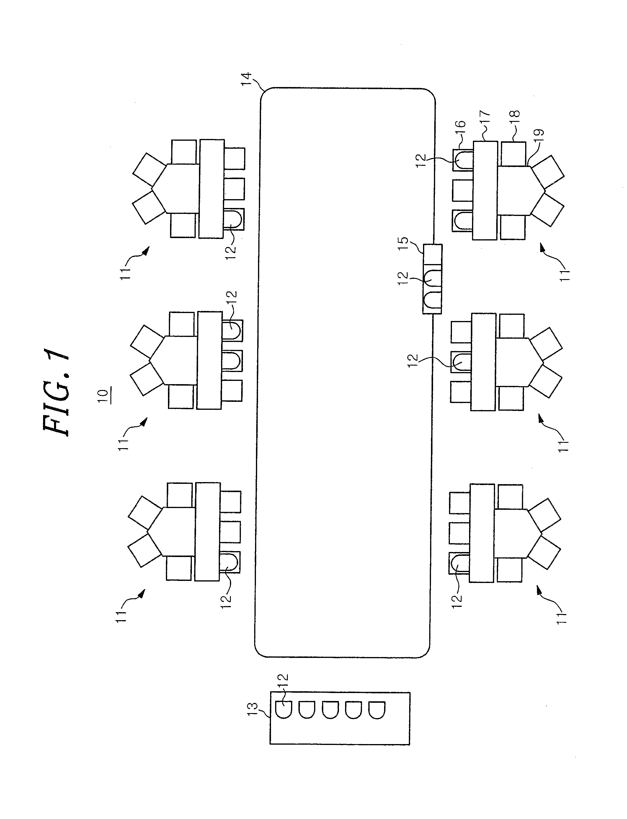
[0025]FIG. 1 is a top view for explaining a substrate processing apparatus for performing a method for setting substrate-treatment time in accordance with an embodiment of the present invention and related devices.

[0026]Referring to FIG. 1, in a clean room 10 of a semiconductor device manufacturing factory, there are provided six substrate processing apparatuses 11, a stocker 13 accommodating therein a plurality of carriers 12, and an AMHS (Automated Material Handling System) 15 such as an OHT (Overhead Hoist Transport) or the like which is moved along a guide 14 extending in the vicinity of the substrate processing apparatuses 11 and the vicinity of the stocker 13. Each of the substrate processing apparatuses 11, the stocker 13 and the AMHS 15 can communicate with a host computer (not shown) that is wiredly or wirelessly connected thereto.

[0027]A single carrier 12 a...


PUM


Abstract

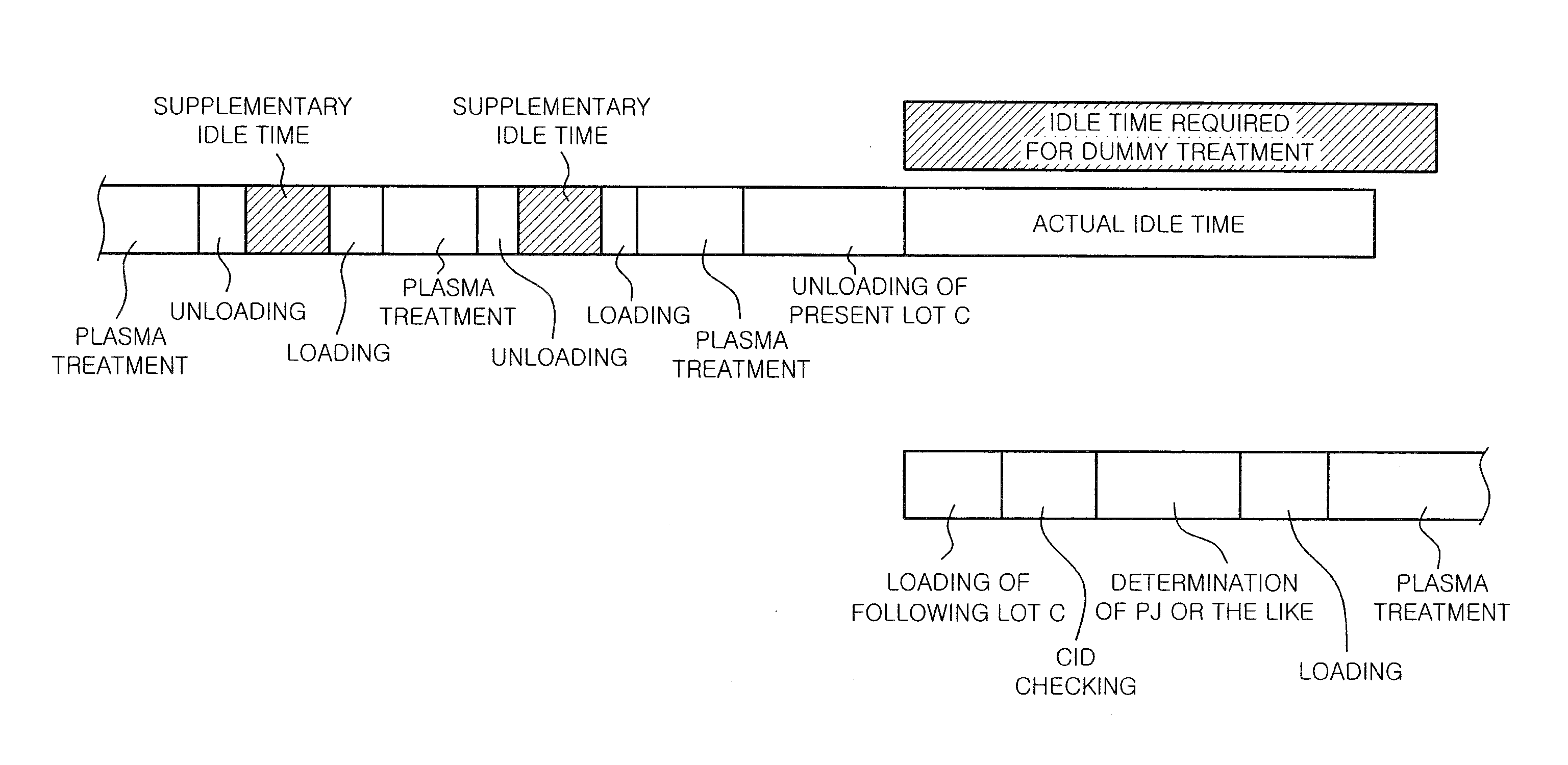
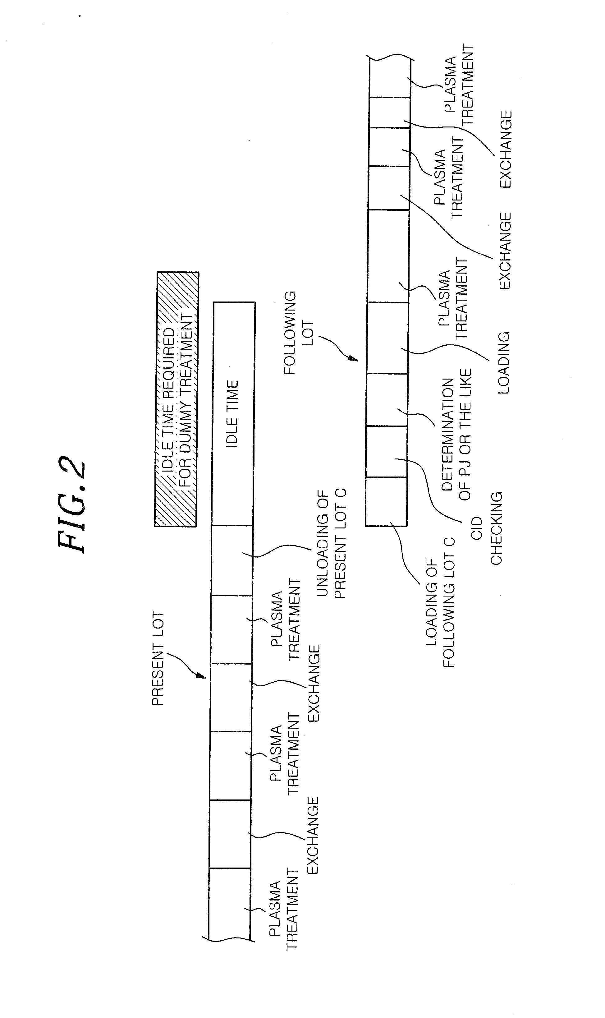
In a method for setting substrate-treatment time, substrate-treatment time is set by the following method. A predicted supply time of wafers of a following lot to a substrate processing apparatus is calculated based on a predicted plasma-treatment completion time of another substrate processing apparatus. A predicted plasma-treatment completion time of all of wafers of a present lot is calculated. A predicted idle time after the completion of the plasma treatment of all of the wafers of the present lot is calculated based on the predicted supply time of the following lot and the predicted plasma-treatment completion time of the present lot. If the predicted idle time is equal to or longer than the idle time required for dummy treatment, supplementary idle time is added between the plasma treatments of unprocessed wafers of the present lot.

Description

CROSS REFERENCE TO RELATED APPLICATION[0001]This application is a 35 U.S.C. 371 National Phase Entry Application from PCT / JP2012 / 066090, filed Jun. 18, 2012, which claims the benefit of Japanese Patent Application No. 2011-140459, filed Jun. 24, 2011, the disclosures of which are incorporated herein in their entirety by reference.FIELD OF THE INVENTION[0002]The present invention relates to a method for setting substrate-treatment time and a storage medium.BACKGROUND OF THE INVENTION[0003]In a substrate processing apparatus for performing plasma treatment, e.g., dry etching or film formation, on a semiconductor device wafer (hereinafter, simply referred to as “wafer”) as a substrate, a single lot including a plurality of, e.g., 25, wafers is supplied while being accommodated in a container (carrier). Further, in the substrate processing apparatus, wafers are taken one by one from the supplied carrier to be subjected to plasma treatment.[0004]In order to manufacture a semiconductor de...

Claims


Application Information

Patent Timeline
Patent Type & Authority Patents(United States)
IPC IPC(8): G05B19/418
CPCG05B19/41865G05B2219/31429G05B2219/45031Y02P90/20Y02P90/02H01L21/67276
Inventor WAKABAYASHI, SHINJI
Owner TOKYO ELECTRON LTD
Learn More