Capacitor arrangement structure and method of mounting capacitor

a technology of arrangement structure and capacitor, which is applied in the direction of printed capacitor incorporation, printed circuit non-printed electric component association, final product manufacture, etc., can solve the problem of difficulty in suppressing the bias of an electric current flowing to each of the capacitors

Active Publication Date: 2016-07-19
TOYOTA JIDOSHA KK
View PDF22 Cites 0 Cited by
  • Summary
  • Abstract
  • Description
  • Claims
  • Application Information

AI Technical Summary

Benefits of technology

[0006]When an electric current is smoothed by dividing between a plurality of capacitors, it is difficult to suppress a bias of an electric current flowing to each of the capacitors. The present invention provides a capacitor arrangement structure that can suppress a bias of an electric current that flows to each of capacitors, and a method of mounting capacitors.
[0009]According to the present invention, a bias of an electric current that flows to each of the capacitors can be suppressed.

Problems solved by technology

When an electric current is smoothed by dividing between a plurality of capacitors, it is difficult to suppress a bias of an electric current flowing to each of the capacitors.

Method used


Image

  • Capacitor arrangement structure and method of mounting capacitor
  • Capacitor arrangement structure and method of mounting capacitor
  • Capacitor arrangement structure and method of mounting capacitor

Examples


first embodiment

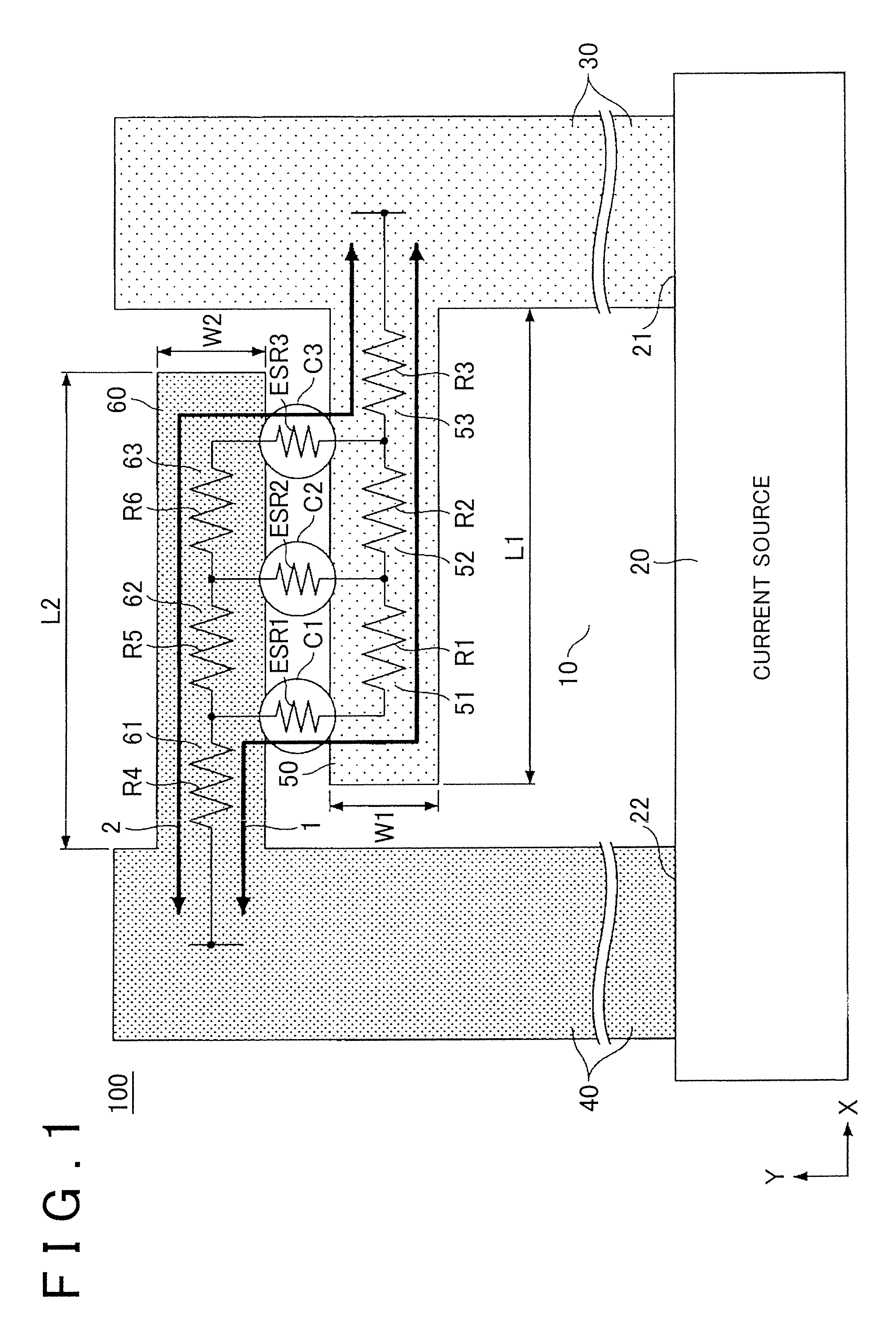
[0016]FIG. 1 is a plan view that schematically shows a configuration example of a capacitor arrangement structure 100 of a The capacitor arrangement structure 100 is a circuit structure that includes a substrate 10; a current source 20 formed on the substrate 10; a conductor pattern formed on the substrate 10; and a plurality of capacitors (three capacitors C1, C2 and C3 are illustrated in FIG. 1) mounted on the substrate 10. The current source 20 is a generator of electric currents that flow to the conductor pattern and a plurality of capacitors, which are formed on the substrate 10. The capacitor arrangement structure 100 includes a wiring pattern 30, a wiring pattern 40, an electrode pattern 50 and an electrode pattern 60, as conductor patterns formed on a surface of the substrate 10.

[0017]The capacitor arrangement structure 100 includes the wiring pattern 30 as a first wiring pattern, and the wiring pattern 40 as a second wiring pattern having a potential different from that of...

second embodiment

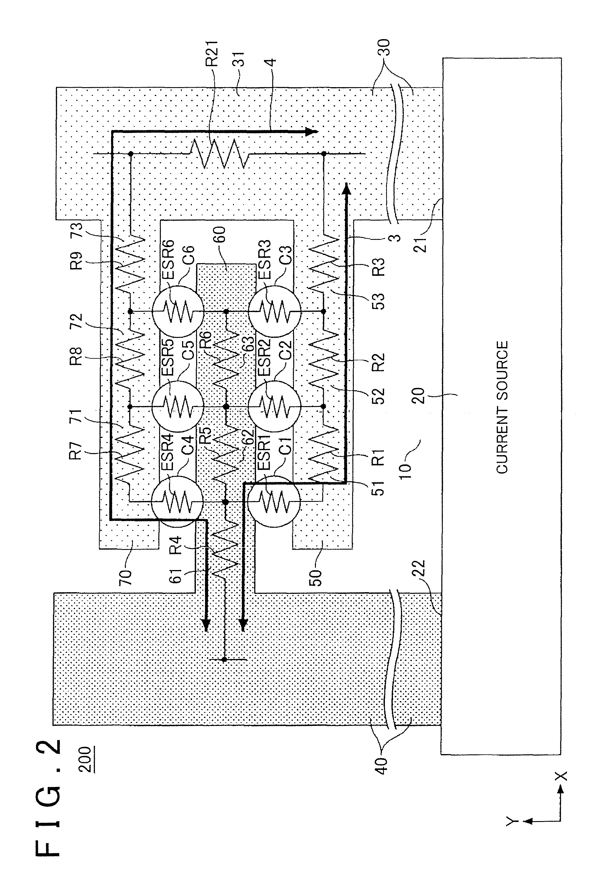
[0034]FIG. 2 is a plan view that schematically shows a configuration example of a capacitor arrangement structure 200 according to a Since the embodiment of FIG. 2 has the same configuration and effects as the embodiment described above, description of the configuration and effects will be omitted or simplified. The capacitor arrangement structure 200 of FIG. 2 has a plurality of electrode patterns that protrudes from at least one wiring pattern formed in a pectinate shape.

[0035]The capacitor arrangement structure 200 is a circuit structure that includes the substrate 10, the current source 20 formed on the substrate 10, a conductor pattern formed on the substrate 10, and a plurality of capacitors (6 capacitors C1 to C6 are illustrated in FIG. 2) mounted on the substrate 10. The capacitor arrangement structure 200 includes, as the conductor pattern formed on a surface of the substrate 10, the wiring pattern 30, the wiring pattern 40, the electrode pattern 50, the electrode pattern ...

third embodiment

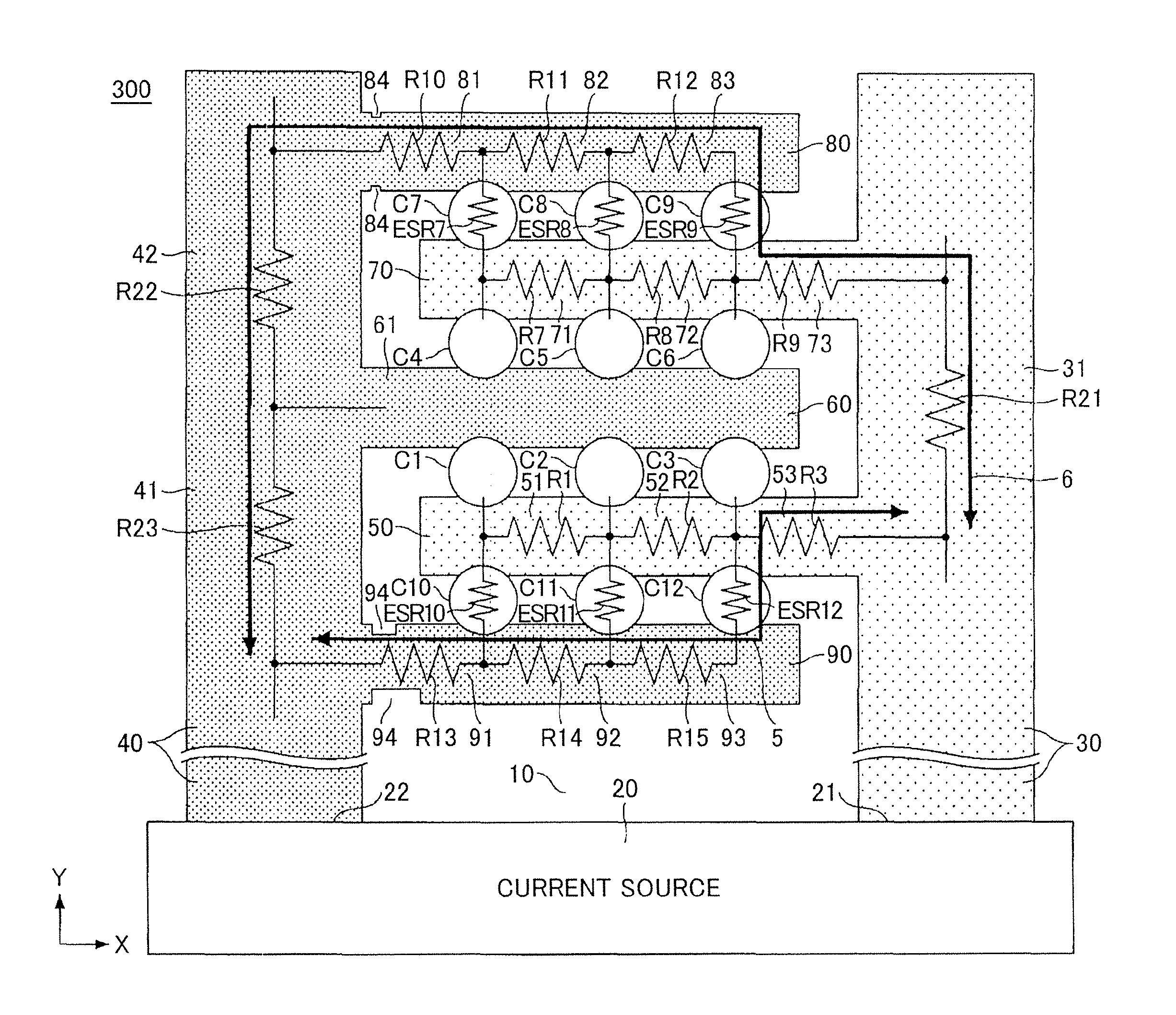
[0062]FIG. 5 is a plan view that schematically shows a configuration example of a capacitor arrangement structure 300 according to a Since the embodiment of FIG. 5 has the same configuration and effects as the embodiments described above, description of the configuration and effects will be omitted or simplified. The capacitor arrangement structure 300 of FIG. 5 has a plurality of electrode patterns protruding from both of wiring patterns alternately, which run in parallel, formed in pectinate shape. The capacitor arrangement structure 300 has a configuration obtained by adding electrode patterns 80 and 90 and capacitors C7 to C12 to the configuration of FIG. 2. In FIG. 5, a part of configuration that duplicates with FIG. 2 is omitted.

[0063]The electrode pattern 90 is an electrode pattern that has a shortest conductor path length on the wiring pattern 40 from the low potential end 22 of the current source 20 to a protruded site among a plurality of electrode patterns 60, 80 and 90 ...


PUM

PropertyMeasurementUnit
resistanceaaaaaaaaaa
resistancesaaaaaaaaaa
lengthaaaaaaaaaa

Abstract

A capacitor arrangement structure includes: a first wiring pattern; a second wiring pattern; a first electrode pattern that protrudes from the first wiring pattern toward the second wiring pattern; a second electrode pattern that protrudes from the second wiring pattern toward the first wiring pattern so as to run in parallel to the first electrode pattern; and a plurality of capacitors that are arranged in parallel between the first electrode pattern and the second electrode pattern.

Description

INCORPORATION BY REFERENCE[0001]The disclosure of Japanese Patent Application No. 2013-124922 filed on Jun. 13, 2013 including the specification, drawings and abstract is incorporated herein by reference in its entirety.BACKGROUND OF THE INVENTION[0002]1. Field of the Invention[0003]The present invention relates to a technique for arranging capacitors between wiring patterns.[0004]2. Description of Related Art[0005]For example, Japanese Patent Application Publication No. 07-175076 (JP No. 07-175076 A) discloses a structure for equalizing wiring resistance values of many wirings in a liquid crystal display element.SUMMARY OF THE INVENTION[0006]When an electric current is smoothed by dividing between a plurality of capacitors, it is difficult to suppress a bias of an electric current flowing to each of the capacitors. The present invention provides a capacitor arrangement structure that can suppress a bias of an electric current that flows to each of capacitors, and a method of mounti...

Claims


Application Information

Patent Timeline
Patent Type & Authority Patents(United States)
IPC IPC(8): H05K1/18H05K3/30H05K1/16H05K1/02H05K1/11H05K3/24
CPCH05K1/181H05K1/165H05K1/162H05K1/0296H05K1/11H05K1/0298H05K3/247H05K2201/0305H05K2201/09236H05K2201/09254H05K2201/09727H05K2201/09736H05K2201/0979H05K2201/10015H05K2201/10522H05K2203/043Y10T29/43Y02P70/611Y02P70/50
Inventor MUTO, JUN
Owner TOYOTA JIDOSHA KK
Why Eureka
Try Eureka