Semiconductor memory device mapping external address as internal address wherein internal addresses of spare cells of two blocks differ by upper most bit and internal addresses of main cells of two blocks differ by upper most bit and the internal addresses of main cell and spare cell of each block differ by one bit and operating method for the same

a memory device and internal address technology, applied in the field of semiconductor memory devices, can solve the problems of large deterioration of the overall performance of the non-volatile semiconductor memory device, difficult to perform the ‘half page read operation’ in burst mode, and achieve the effect of efficient address mapping

Active Publication Date: 2016-09-13
SK HYNIX INC
View PDF21 Cites 0 Cited by
  • Summary
  • Abstract
  • Description
  • Claims
  • Application Information

AI Technical Summary

Benefits of technology

[0023]An embodiment of the present invention is directed to an address mapping circuit that performs an efficient address mapping operation thereby supporting access of memory cell array in a burst mode as well as common column address decoding operation without increasing the size of a semiconductor memory device, the memory cell array of which is divided into multiple regions according to addresses, and an operating method for the address mapping circuit.

Problems solved by technology

However, according to the structure of the prior art shown in FIG. 1, where the pages of the memory cell array are sequentially disposed in the order of the main even page MAIN_EVEN (1), the main odd page MAIN_ODD (2), the spare even page SPARE_EVEN (3), and the spare odd page SPARE_ODD (4), it is hard to perform the ‘half page read operation’ in a burst mode.
In other words, it is hard to realize the half page read operation according to the structure of the prior art shown in FIG. 1 in the burst mode.
Thus, great deterioration of the overall performance of the non-volatile semiconductor memory device may occur.
According to the prior art shown in FIG. 2, however, the column address scheme becomes different as well, and it is impossible to perform the common column address decoding operation of the prior art shown in FIG. 1.
Because of the impossibility of the common column address decoding operation, the column decoding operation has to be performed separately for the even page and for the odd page, which causes needs for independent elements that respectively decode the even page and the odd page, and thus creating the need for double sized column decoding unit.
This increases the chip size.
Therefore, the prior art shown in FIG. 2 may not be a solution to the half page read operation in the burst mode.

Method used


Image

  • Semiconductor memory device mapping external address as internal address wherein internal addresses of spare cells of two blocks differ by upper most bit and internal addresses of main cells of two blocks differ by upper most bit and the internal addresses of main cell and spare cell of each block differ by one bit and operating method for the same
  • Semiconductor memory device mapping external address as internal address wherein internal addresses of spare cells of two blocks differ by upper most bit and internal addresses of main cells of two blocks differ by upper most bit and the internal addresses of main cell and spare cell of each block differ by one bit and operating method for the same
  • Semiconductor memory device mapping external address as internal address wherein internal addresses of spare cells of two blocks differ by upper most bit and internal addresses of main cells of two blocks differ by upper most bit and the internal addresses of main cell and spare cell of each block differ by one bit and operating method for the same

Examples


Embodiment Construction

[0045]Exemplary embodiments of the present invention will be described below in more detail with reference to the accompanying drawings. The present invention may, however, be embodied in different forms and should not be construed as limited to the embodiments set forth herein. Rather, these embodiments are provided so that this disclosure will be thorough and complete, and will fully convey the scope of the present invention to those skilled in the art. Throughout the disclosure, reference numerals correspond directly to the like numbered parts in the various figures and embodiments of the present invention. In addition, a singular form may include a plural form as long as it is not specifically mentioned in a sentence.

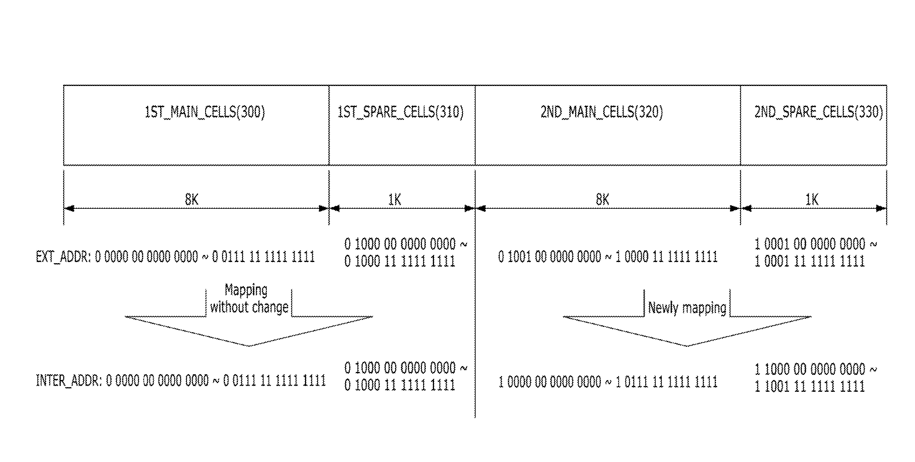
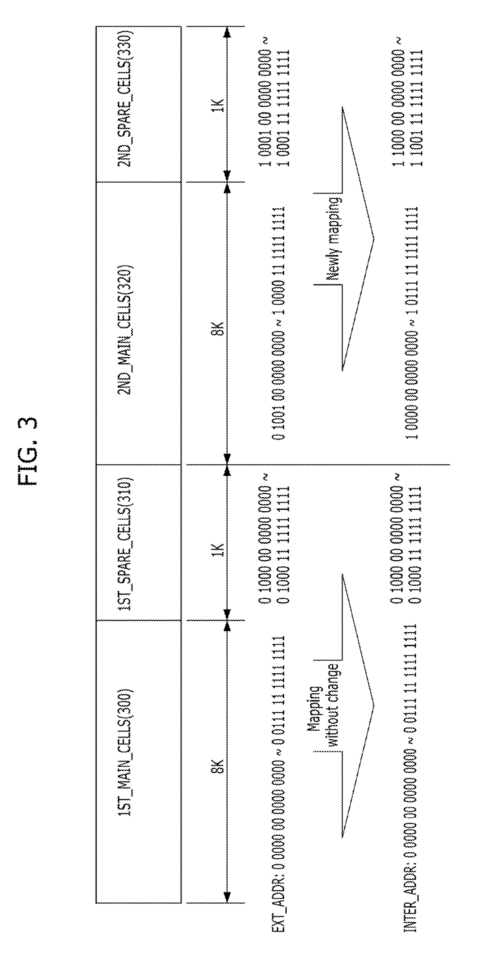
[0046]According to an embodiment of the present invention, two address schemes for access to memory cell arrays in a semiconductor memory device are provided. First scheme is for an external address used in the outside of the device. The external address correspondi...


PUM


Abstract

Provided is a semiconductor memory device that may efficiently map an internal address used inside the semiconductor memory device in response to an external address that is applied from the outside of the semiconductor memory device. The semiconductor memory device may include a memory cell array configured to include a first main cell array, a first spare cell array, a second main cell array, and a second spare cell array each of which has internal cells that are selected in response to an internal address, and an address mapping unit configured to map external address as the internal address when the external address designates the first main and spare cell arrays, and to operate calculation with a given value and the external address and to map the calculation result value as the internal address when the external address designates the second main and spare cell arrays.

Description

CROSS-REFERENCE TO RELATED APPLICATIONS[0001]The present application claims priority of Korean Patent Application No. 10-2012-0155059, filed on Dec. 27, 2012, which is incorporated herein by reference in its entirety.BACKGROUND[0002]1. Field[0003]Exemplary embodiments of the present invention relate to a semiconductor designing technology, and more particularly, to a semiconductor memory device that may efficiently map an internal address internally used in the memory cell array of the semiconductor memory device in response to an external address that is applied from the outside of the semiconductor memory device.[0004]2. Description of the Related Art[0005]Semiconductor memory devices are generally divided into volatile semiconductor memory devices and non-volatile semiconductor memory devices. Recently, there are increasing demands for the non-volatile memory devices that are capable of performing program and erase operations without a refresh operation, which is an operation of ...

Claims


Application Information

Patent Timeline
Patent Type & Authority Patents(United States)
IPC IPC(8): G11C29/00
CPCG11C29/84G11C29/82G11C8/04
Inventor LIM, SANG-OH
Owner SK HYNIX INC
Why Eureka
Try Eureka