
Power semiconductor device and corresponding module

a technology of semiconductor devices and modules, applied in the field of power electronics, can solve the problems of reduced thyristor structure enhancement effect, limited short circuit capability of devices, and high on-state losses, and achieves improved carrier enhancement at the emitter, good mos controllability, and low on-state losses.

Inactive Publication Date: 2016-09-27
ABB (SCHWEIZ) AG
View PDF5 Cites 2 Cited by
  • Summary
  • Abstract
  • Description
  • Claims
  • Application Information

AI Technical Summary

Benefits of technology

[0009]It is an object of the invention to provide a power semiconductor device, which provides lower on-state losses by having better carrier enhancement at the emitter, while having good MOS controllability and higher safe operating area than prior art devices, in particular EST devices.
[0021]Due to the introduction of additional IGBT channel the device has less drainage effect and the IGBT and Thyristor sections can be optimized independently depending on the electrical and geometrical requirements. The parallel IGBT provides options for gate driving and improved turn-off capability. Also the MOS channel can be designed independently so that the device provides low losses.
[0022]Due to the different channels, the device provides a high level of carrier enhancement at the emitter and lower hole drainage, hence the on state losses are reduced.
[0023]Due to the enhancement layer 52, there is an improvement in plasma distribution, current enhancement at the IGBT channel and improved latch up properties so that on state losses are reduced. High doping concentrations of the enhancement layer can be chosen for improved carrier enhancement.

Problems solved by technology

Such a device has limited short circuit capability depending on its low voltage MOSFET blocking and higher on-state snapback effects.
Also the on-state losses are higher due to the low voltage MOSFET channel resistance than for a prior art IGCT.
The base layer is shorted in the EST devices, so that the thyristor structure enhancement effect is reduced due to hole drainage, and hence this results in higher on-state losses.
Such a device results in high on-state losses due to a strong contribution of the IGBT drainage.

Method used


Image

  • Power semiconductor device and corresponding module
  • Power semiconductor device and corresponding module
  • Power semiconductor device and corresponding module

Examples


Embodiment Construction

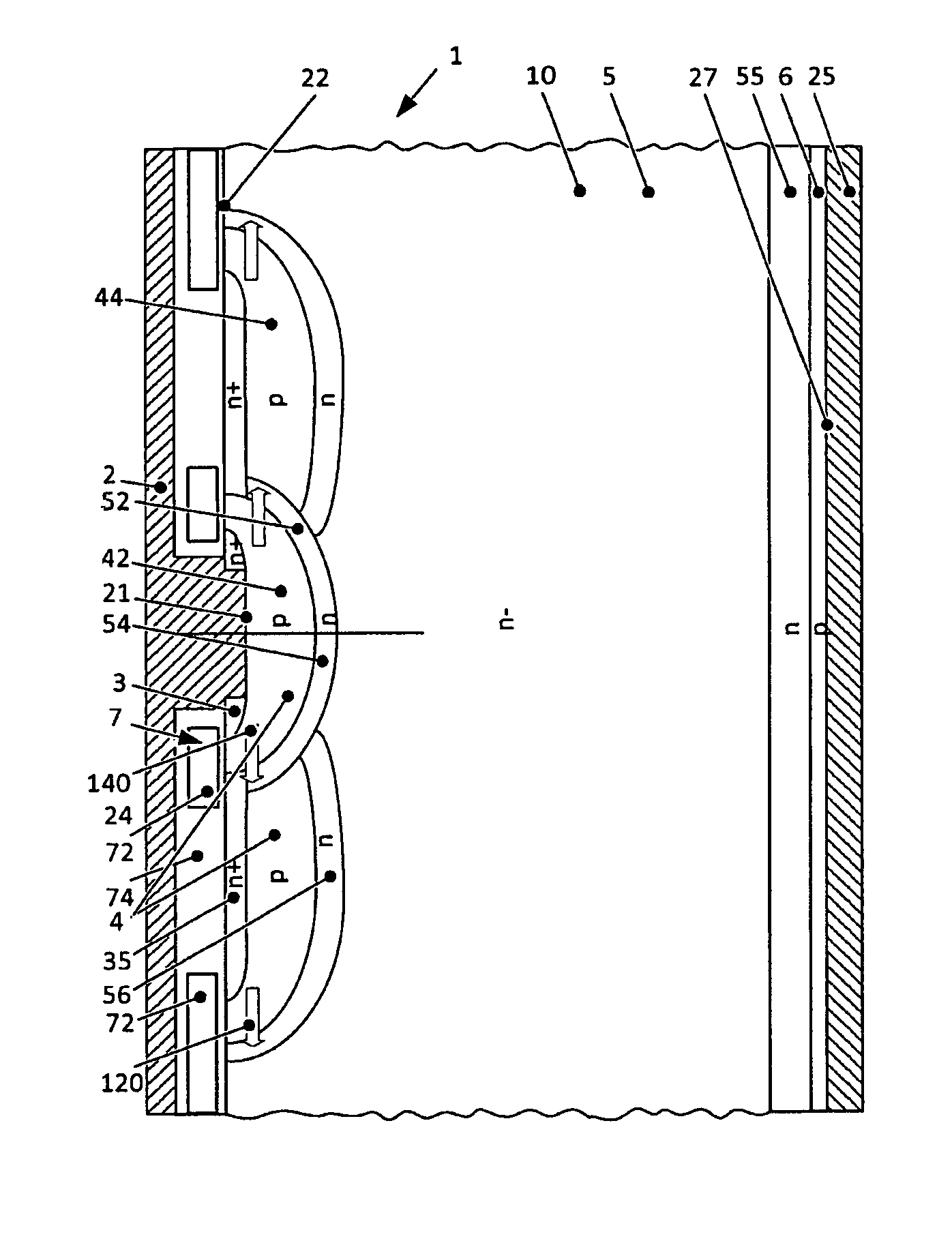
[0033]An inventive power semiconductor device 1 as shown in FIG. 2 comprises a wafer 10, on which wafer 10 an emitter electrode 2 is arranged on an emitter side 22 of the wafer and a collector electrode 25 is arranged on a collector side 27 of the wafer opposite to the emitter side 22. FIG. 2A shows a top view on the device 1, whereas FIG. 2B shows a cut along the line B-B in FIG. 2A and FIG. 2C show a cut along the line A-A in FIG. 2A. FIGS. 3A-5C show the same views for different inventive devices, whereas FIG. 6 shows a cut along the line B-B in FIG. 2A at a shifted section of the device.

[0034]The wafer comprises n and p doped layers between the collector side 27 and the emitter side 22 in the following order: a p doped collector layer 6, a constantly low (n−) doped drift layer 5, an n doped enhancement layer 52, which has a higher maximum doping concentration than the drift layer 5 and which comprises a first enhancement region 54, a p doped base layer 4, which comprises a first...


PUM


Abstract

Power semiconductor device having a wafer, including emitter and collector electrodes arranged on opposite sides, wherein a gate electrode arranged on the emitter side has a conductive gate layer and an insulating layer arranged in the following order between the collector and emitter side: a p doped collector layer, an (n−) doped drift layer, an n doped enhancement layer, a p based base layer having a first and second base region, and an (n+) doped first and second emitter layer, wherein the emitter electrode contacts the first emitter layer and the first base region at an emitter contact area, wherein the second emitter layer is insulated from a direct contact to the emitter electrode by the insulating layer and wherein the second emitter layer is separated from the first emitter layer by the base layer.

Description

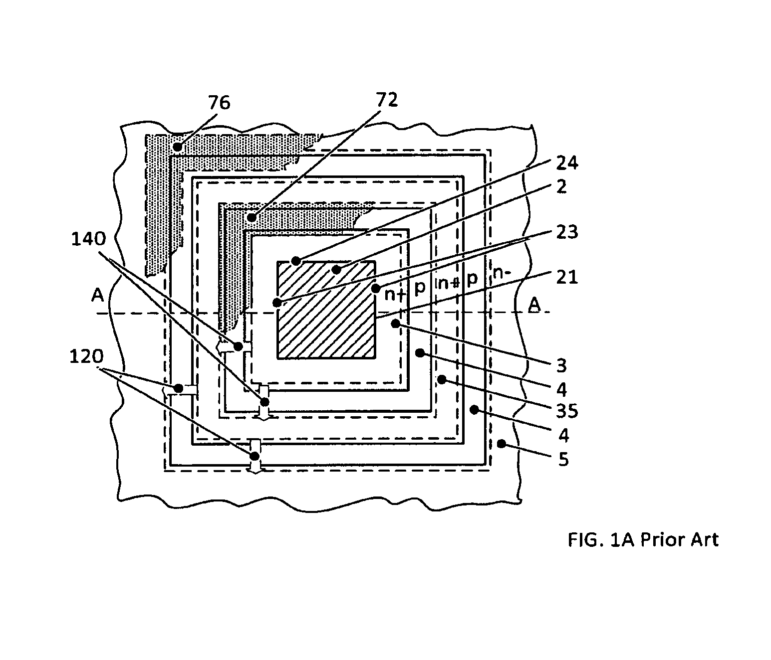
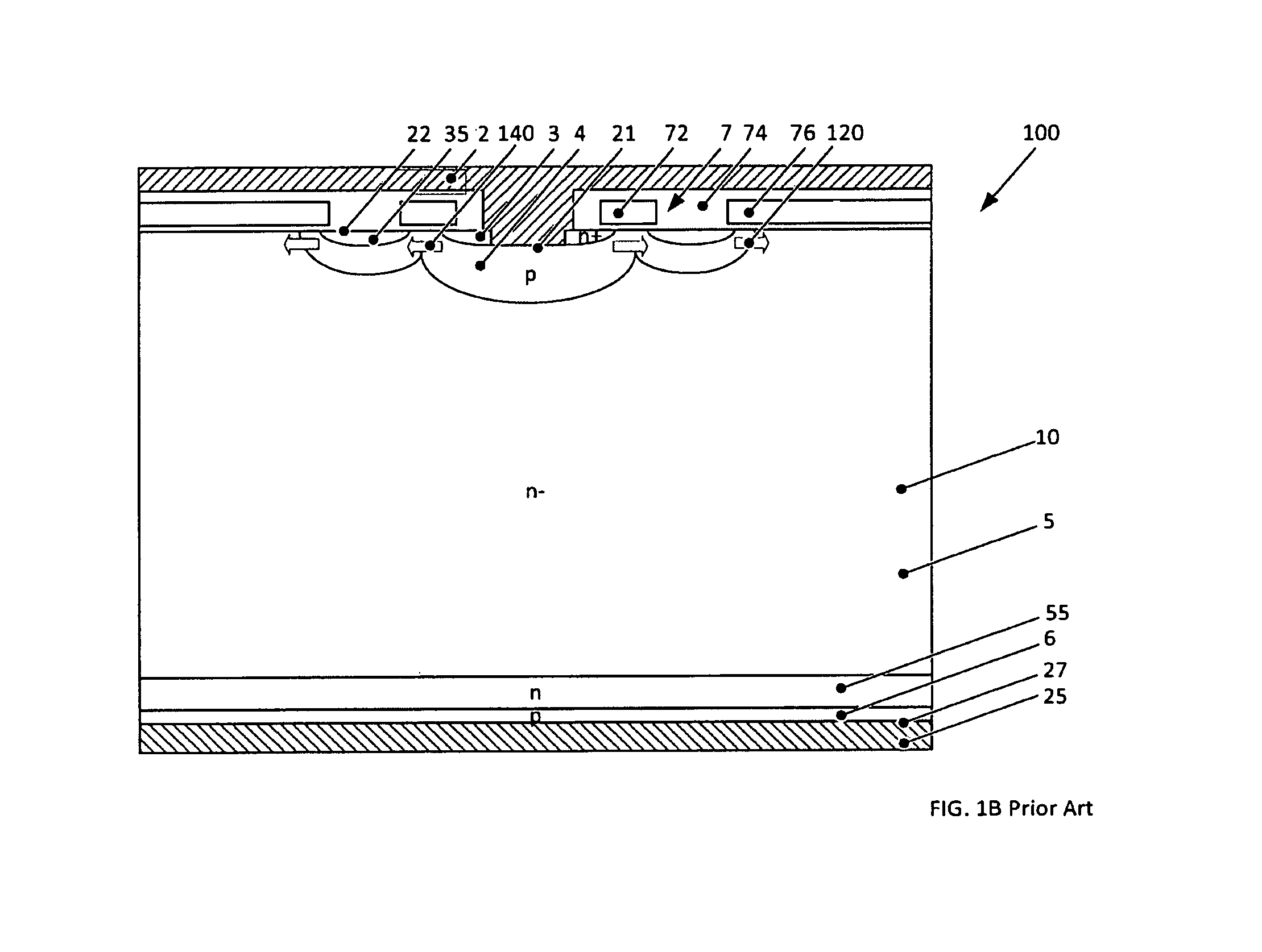
FIELD OF THE INVENTION[0001]The invention relates to the field of power electronics and more particularly to a power semiconductor device.BACKGROUND OF THE INVENTION[0002]In FIG. 1A and FIG. 1B an emitter switched thyristor (EST) 100 is shown, which comprises a wafer 10 having an emitter and a collector side 22, 27, on which sides an emitter electrode 2 and a collector electrode 25 are arranged. On the emitter side 22, a planar or trench gate electrode 7 is arranged, which comprises an electrically conductive gate layer 72, a further gate layer 76 and an insulating layer 74, which insulates the gate layer 72 and 76 from any layer of the first or second conductivity type in the wafer 10 and from each other. FIG. 1A shows a top view on the device 100, whereas FIG. 1B shows a cut along the line A-A in FIG. 1A.[0003]Like in an IGBT, on the emitter side 22, an n doped first emitter layer 3, which extends to a region below the gate layer 72 and a p doped base layer 4 surrounding the first...

Claims


Application Information

Patent Timeline
Patent Type & Authority Patents(United States)
IPC IPC(8): H01L29/739H01L29/417H01L29/10H01L29/08H01L29/745H01L29/749H01L27/06H01L29/06
CPCH01L29/7395H01L27/0623H01L29/083H01L29/0813H01L29/0821H01L29/1004H01L29/1012H01L29/1016H01L29/1095H01L29/41708H01L29/749H01L29/7455H01L29/0696H01L29/102
Inventor RAHIMO, MUNAF
Owner ABB (SCHWEIZ) AG
Learn More