
Super-junction schottky PIN diode

a schottky pin and oxide diode technology, applied in the direction of basic electric elements, electrical equipment, semiconductor devices, etc., can solve the problems of high switching loss, high switching time and high switching loss of pin diodes, so as to reduce forward voltage, reduce switching loss, and reduce switching loss

Active Publication Date: 2016-02-16
ROBERT BOSCH GMBH
View PDF13 Cites 1 Cited by
  • Summary
  • Abstract
  • Description
  • Claims
  • Application Information

AI Technical Summary

Benefits of technology

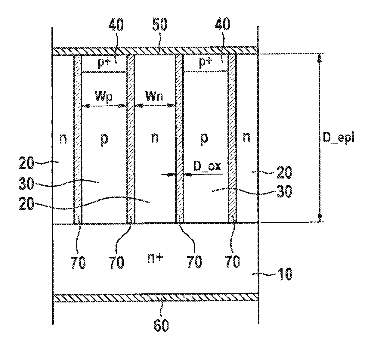
[0010]A high-blocking high-voltage diode having low forward voltage and favorable switching behavior is thus advantageously provided. A diode according to the present invention, also referred to as a super-junction Schottky oxide PIN diode, represents a combination of a Schottky diode with a PIN diode, which together form a superjunction structure and are galvanically separated from one another. In comparison to conventional PIN power diodes having similarly low forward voltages, a diode according to the present invention has much lower switch-off losses.
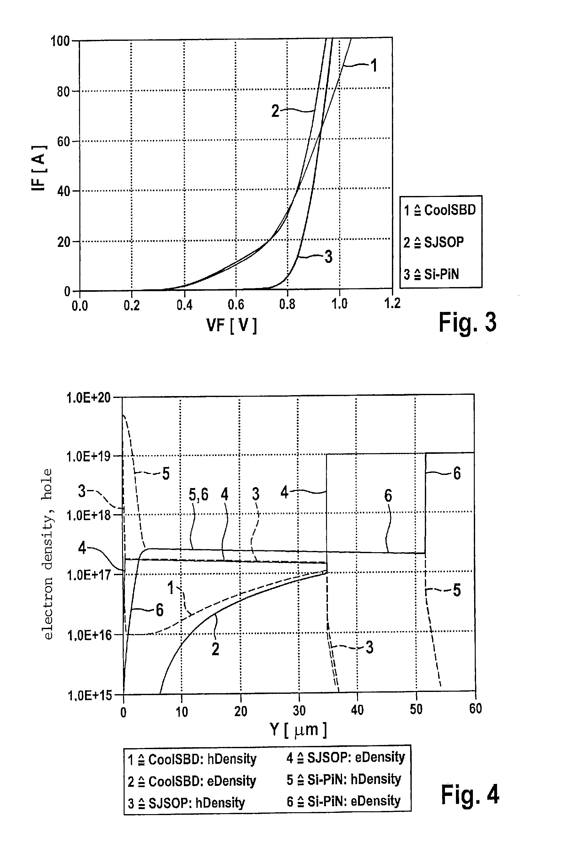
[0012]In comparison to a high-voltage PIN diode, a diode according to the present invention has a much smaller switch-off power loss for a comparable forward voltage and high current densities.
[0013]Compared to a Cool SBD, a diode according to the present invention has a lower forward voltage at high current density, and only a negligibly higher switch-off power loss.

Problems solved by technology

However, high switching losses, which occur as switch-off losses during current commutation, are disadvantageous.
A higher drain current means a higher switch-off power loss.
Switching times and switching losses are high for PIN diodes.
However, for high blocking voltages, thick semiconductor layers with low-level doping are once again necessary, which for high currents results in unacceptable high forward voltages.
For this reason, power Schottky diodes implemented in silicon technology, despite good switching behavior, are not suitable for blocking voltages above approximately 100 V.
However, the low forward voltage of the PIN diode is not achieved for high currents.

Method used


Image

  • Super-junction schottky PIN diode
  • Super-junction schottky PIN diode
  • Super-junction schottky PIN diode

Examples


Embodiment Construction

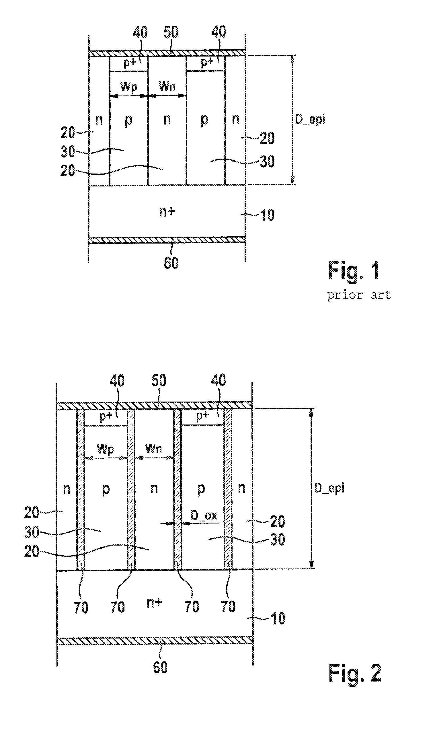
[0024]FIG. 1 illustrates a detail of the structure of a Cool SBD corresponding to the related art, in cross section. The Cool SBD is composed of an n+ substrate 10 on which an n-epilayer 20 having thickness D_epi and doping concentration ND is arranged. n-epilayer 20 contains etched-in trenches 30 which are filled with p-doped silicon having doping concentration NA, and which in the upper regions are filled with p+-doped silicon 40. The width of n regions 20 is Wn, and the width of p and p+ regions 30 and 40, respectively, is Wp. Dopings and widths are selected in such a way that the regions are depleted when the full blocking voltage is applied (superjunction principle). This is the case, for example, for NA·Wp=ND·Wn=1012 cm−2. On the front side of the chip, n-doped regions 20 and p+-doped regions 40 are covered by a continuous first metal layer 50, which with n-doped regions 20 forms a Schottky contact, and with p+-doped regions 40 forms an ohmic contact. Metal layer 50 represents...


PUM


Abstract

A semiconductor chip has an n+-doped substrate, above which an n-doped epilayer having trenches is introduced, the trenches being filled with p-doped semiconductor material and in each case having a highly p-doped region at their top side, such that an alternating arrangement of n-doped regions having a first width and p-doped regions having a second width is present. A first metal layer functioning as an anode is provided on the front side of the chip and forms a Schottky contact with the n-doped epilayer and forms an ohmic contact with the highly p-doped regions. A second metal layer which represents an ohmic contact and functioning as a cathode is formed on the rear side of the semiconductor chip. A dielectric layer is provided between each n-doped region and an adjacent p-doped region.

Description

BACKGROUND OF THE INVENTION[0001]1. Field of the Invention[0002]The present invention relates to a super-junction Schottky PIN oxide diode.[0003]2. Description of the Related Art[0004]Increasingly efficient current converters are becoming necessary with regard to issues associated with CO2 emissions. Examples include inverters for photovoltaic or automotive applications. To this end, highly blocking, low-loss, quickly switching power semiconductors are necessary. In addition to active semiconductor switches such as IGBTs or CoolMOS transistors, freewheeling diodes are also required. For high-voltage applications, PIN diodes made of silicon are generally used. PIN diodes have small conducting-state voltages and low blocking currents, and therefore have low forward losses and blocking losses. However, high switching losses, which occur as switch-off losses during current commutation, are disadvantageous.[0005]High-voltage PIN diodes are PN diodes in which an undoped (intrinsic), and i...

Claims


Application Information

Patent Timeline
Patent Type & Authority Patents(United States)
IPC IPC(8): H01L29/872H01L29/06H01L29/66H01L29/868
CPCH01L29/0649H01L29/66143H01L29/868H01L29/872H01L29/0634
Inventor QU, NINGGOERLACH, ALFRED
Owner ROBERT BOSCH GMBH
Learn More