Organic light-emitting display device and method for manufacturing organic light-emitting display device

a technology of manufacturing method, which is applied in sustainable manufacturing/processing, identification means, instruments, etc., can solve the problems of easy cracks in wiring in the bending area, difficult to minimize the cracks in the wiring, and increased so as to minimize the failure of the organic light-emitting display device, the effect of increasing the stress on the bending area

Active Publication Date: 2016-11-08
LG DISPLAY CO LTD
View PDF5 Cites 12 Cited by
  • Summary
  • Abstract
  • Description
  • Claims
  • Application Information

AI Technical Summary

Benefits of technology

[0007]When the flexible substrate of the organic light-emitting display device is bent, stress is exerted to a bending area of the flexible substrate. The flexible substrate may be not bent in an intended bending direction, that is, the bending direction thereof may be deviated. At this time, the stress exerted to the bending area is more increased, and, thus, cracks in a wiring in the bending area may easily occur. Accordingly, in order to minimize failures of the organic light-emitting display device due to the cracks in the wiring to improve reliability of the organic light-emitting display device, the present disclosure describes an organic light-emitting display device enabling accurate bending of the flexible substrate in the intended bending direction, and a method for manufacturing the same.
[0008]An object of the present disclosure is to provide an organic light-emitting display device with minimization of cracks occurrences in a wiring in a bending area for a flexible substrate bending, and a method for manufacturing the same.
[0010]According to an aspect of the present disclosure, there is provided an organic light-emitting display device with a flexible substrate bent across a bend line. The flexible substrate of the organic light-emitting display device includes a first area, a first bending area adjacent to the first area, a second bending area adjacent to the first bending area, and a second area adjacent to the second bending area. The flexible substrate is bent such that the first area is positioned to at least partially overlap the second area and the first bending area is positioned to at least partially overlap the second bending area. A wiring unit is formed across the first area, the first bending area, the second bending area, and the second area of the flexible substrate. The wiring unit is configured to electrically connect together a display unit formed in the first area of the flexible substrate and a pad unit formed in the second area of the flexible substrate. A first alignment key is formed over the flexible substrate and a second alignment key is formed over the flexible substrate. The first alignment key is positioned to overlap the second alignment key with the flexible substrate bent across the bend line. The wiring formed at the flexible substrate is also bent along with the bending of the flexible substrate. Cracks may occur in the bent wiring, and in order to minimize the crack occurrence, a shape of the wiring is designed in consideration of a bending direction of the flexible substrate. However, even though the shape of the wiring is designed in consideration of a bending direction of the flexible substrate, when the flexible substrate is not accurately bent in an intended bending direction, it is difficult to minimize the crack occurrence in the wiring. Accordingly, by bending the flexible substrate to allow the first alignment key and the second alignment key to face each other, it is possible to accurately bend the flexible substrate in the intended bending direction and to minimize the cracks occurring in the wiring.
[0011]According to another aspect of the present disclosure, there is provided a method for manufacturing an organic light-emitting display device which can bend a flexible substrate of the organic light-emitting display device in an intended bending direction. The method for manufacturing an organic light-emitting display device includes securing the flexible substrate to a stage, bending the flexible substrate in the first bending area and the second bending area, clamping the second area of the bent flexible substrate using a clamp, aligning the first alignment key to overlap with the second alignment key by moving the stage or clamp until the first alignment key overlaps the second alignment key, and pressing the flexible substrate until the first area of the flexible substrate is in contact with the second area of the flexible substrate. By matching the first alignment key to the second alignment key, the flexible substrate can be accurately bent in the intended bending direction.

Problems solved by technology

At this time, the stress exerted to the bending area is more increased, and, thus, cracks in a wiring in the bending area may easily occur.
However, even though the shape of the wiring is designed in consideration of a bending direction of the flexible substrate, when the flexible substrate is not accurately bent in an intended bending direction, it is difficult to minimize the crack occurrence in the wiring.

Method used


Image

  • Organic light-emitting display device and method for manufacturing organic light-emitting display device
  • Organic light-emitting display device and method for manufacturing organic light-emitting display device
  • Organic light-emitting display device and method for manufacturing organic light-emitting display device

Examples


Embodiment Construction

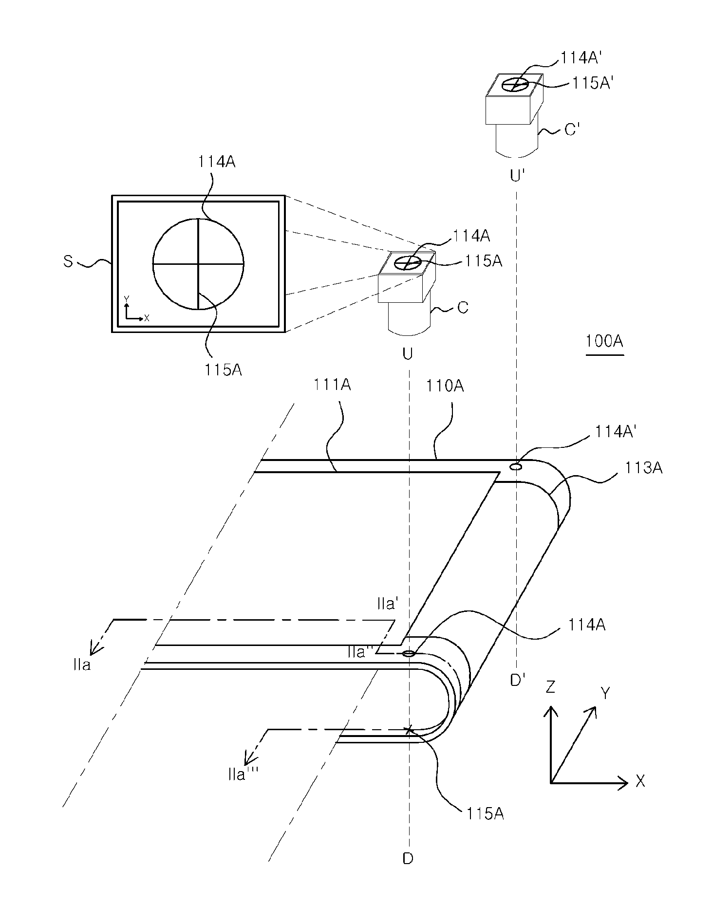
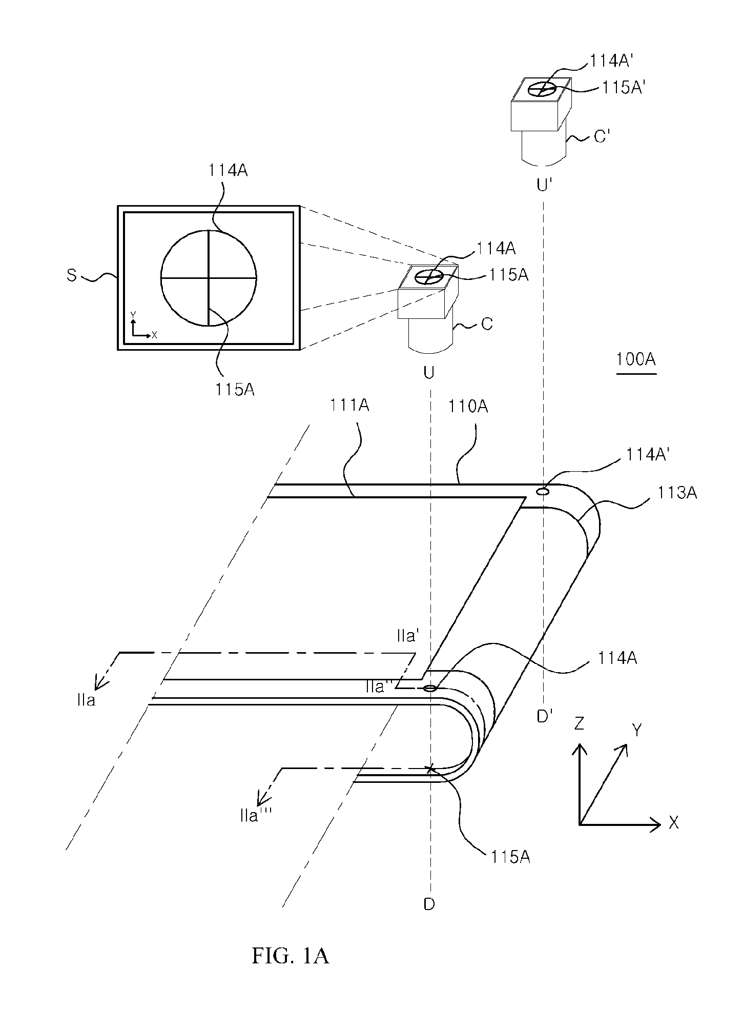
[0025]Various advantages and features of the present disclosure and methods accomplishing thereof will become apparent from the following description of embodiments with reference to the accompanying drawings. However, the present disclosure is not limited to exemplary embodiment disclosed herein but will be implemented in various forms. The exemplary embodiments are provided by way of example only so that a person of ordinary skilled in the art can fully understand the disclosures of the present disclosure and the scope of the present disclosure. Therefore, the present disclosure will be defined only by the scope of the appended claims.

[0026]Indicating that elements or layers are “on” other elements or layers include both a case in which the corresponding elements are just above other elements and a case in which the corresponding elements are intervened with other layers or elements.

[0027]Although first, second, and the like are used for illustrating various components, the compon...


PUM

PropertyMeasurementUnit
stressaaaaaaaaaa
flexibleaaaaaaaaaa
areaaaaaaaaaaa

Abstract

Provided are an organic light-emitting display device and a method for manufacturing the same. A flexible substrate of the organic light-emitting display device is bent across a bend line and includes a first area, a first bending area adjacent to the first area, a second bending adjacent to the first bending area, and a second area adjacent to the second bending area. A wiring is formed over the first area, the first bending area, the second bending area, and the second area of the flexible substrate to electrically connect a display unit formed in the first area and a pad unit formed in the second area. A first alignment key is formed over the flexible substrate, and a second alignment is formed over the flexible substrate. The first alignment key is positioned to overlap the second alignment key with the flexible substrate bent across the bend line.

Description

CROSS-REFERENCE TO RELATED APPLICATIONS[0001]This application claims the priority of Korean Patent Application No. 10-2013-0142545 filed on Nov. 21, 2013 in the Korean Intellectual Property Office, the disclosure of which is incorporated herein by reference.BACKGROUND OF THE DISCLOSURE[0002]Field of the Disclosure[0003]The present disclosure relates to an organic light-emitting display device and a method for manufacturing the same and more particularly, to an organic light-emitting display device with minimization of crack occurrences in a wiring in a flexible substrate via accurate bending of the flexible substrate, and a method for manufacturing the same.[0004]Description of the Related Art[0005]In recent years, a flexible display device has attracted of attention as a next generation display device. Such a flexible device may be capable of displaying an image in a case of a substrate bending like paper via formation of a display unit, a wiring and / or the like on a flexible subst...

Claims


Application Information

Patent Timeline
Patent Type & Authority Patents(United States)
IPC IPC(8): H01L23/544H01L51/56B32B37/14B32B38/00B32B38/18H01L51/00
CPCH01L23/544B32B37/14B32B37/144B32B38/0012B32B38/1833H01L51/0097H01L51/56B32B2307/422B32B2457/206H01L2223/5442H01L2223/54426H01L2223/54486H01L2924/0002Y02E10/549Y02P70/521Y10T156/1051H01L2924/00Y02P70/50H10K77/111G09F9/33H10K59/00H10K50/80H10K71/00
Inventor YANG, HEESEOK
Owner LG DISPLAY CO LTD
Why Eureka
Try Eureka