
Semiconductor device with improved bonding

a technology of semiconductors and semiconductors, applied in the direction of semiconductor devices, semiconductor/solid-state device testing/measurement, semiconductor/solid-state device details, etc., can solve the problems of long processing time, defective bonded parts, and inability to perform bonding steps

Inactive Publication Date: 2004-04-27
KIOXIA CORP
View PDF5 Cites 49 Cited by
  • Summary
  • Abstract
  • Description
  • Claims
  • Application Information

AI Technical Summary

Benefits of technology

The solution improves the reliability and bonding strength of copper wiring layers by forming an alloy layer with metals like Al, Ti, or Ta, reducing oxidation and increasing the durability of the pad electrode layer, thus enhancing the overall performance and longevity of semiconductor devices.

Problems solved by technology

Therefore, when Cu is used as a pad material, the bonding step cannot be performed while heating in the atmosphere by a conventional apparatus.
In a step of heating treatment after the bonding, there is also a problem that a bonded part becomes defective because oxidation continues.
However, if the metal film (e.g., Al) formed on the pad electrode layer is excessively thin, the following problems occur.
In this case, an unnecessary portion of the metal film remained on the insulating film around the pad electrode layer is removed by a wet etching process or a CMP method (=chemical-mechanical polishing method), etc., but there is a problem that the processing time becomes long and a practical process margin cannot be obtained.
In this case, there comes a scratch of certain depth in the pad electrode layer when the pad electrode layer is contacted by the probing needle because it has a sharp tip.
Therefore, when the pad electrode layer has a structure that the protective layer is formed on the Cu wiring layer, the probing needle breaks through the protective layer to reveal the Cu wiring layer located below it, resulting in oxidation in the later assembly step.
Therefore, there is also a problem that a metal oxide layer on the pad electrode layer is readily cut away by the probing needle, and the oxidation resistance of the pad electrode layer is degraded.
However, it is impossible to form the metal oxide layer again because a metal required to form the metal oxide layer as the protective layer is not enough contained in the Cu wiring layer located on a lower layer.
In the assembly step, particularly in the bonding step or the like, a bonding strength and conductivity become defective when the metal wire or conductive bump are connected to such pad electrode.
However, the conventional wiring pad structure has the following problems.
As a result, there is a problem that the wire bonding resistance is degraded or the pad section has a greatly increased resistance.
Besides, when oxidation reaches the deep section of the wiring layer, a problem such as fatal deterioration occurs in the wiring characteristic such as electro-migration (EM) resistance, stress migration (SM) resistance or the like in addition to the aforementioned problem.
Thus, it is probable that the wire bonding resistance is degraded, the resistance of the pad section is increased, and the wiring characteristics such as the EM resistance or the SM resistance are fatally degraded.
However, Al and Cu are highly reactive, so that when the Al cap film is directly stacked on the Cu surface, there is a problem that an intermetallic compound is formed and a resistance is increased by the subsequent major step which is a passivation deposition step or a thermal process such as a connection step by bump connection or wire bonding.
But, there may be a problem that the barrier metal film having a general laminated structure formed of two layers of Ta.sub.2 N and Ta is sheared due to delamination caused when probing.
In the barrier metal forming process, there may be a problem that dust (particles) increases in the sputtering step when a layer of Ta.sub.2 N of the Ta-based barrier metal is made thick, and the barrier properties are degraded due to existance of the dust.

Method used


Image

  • Semiconductor device with improved bonding
  • Semiconductor device with improved bonding
  • Semiconductor device with improved bonding

Examples


first embodiment

(First Embodiment)

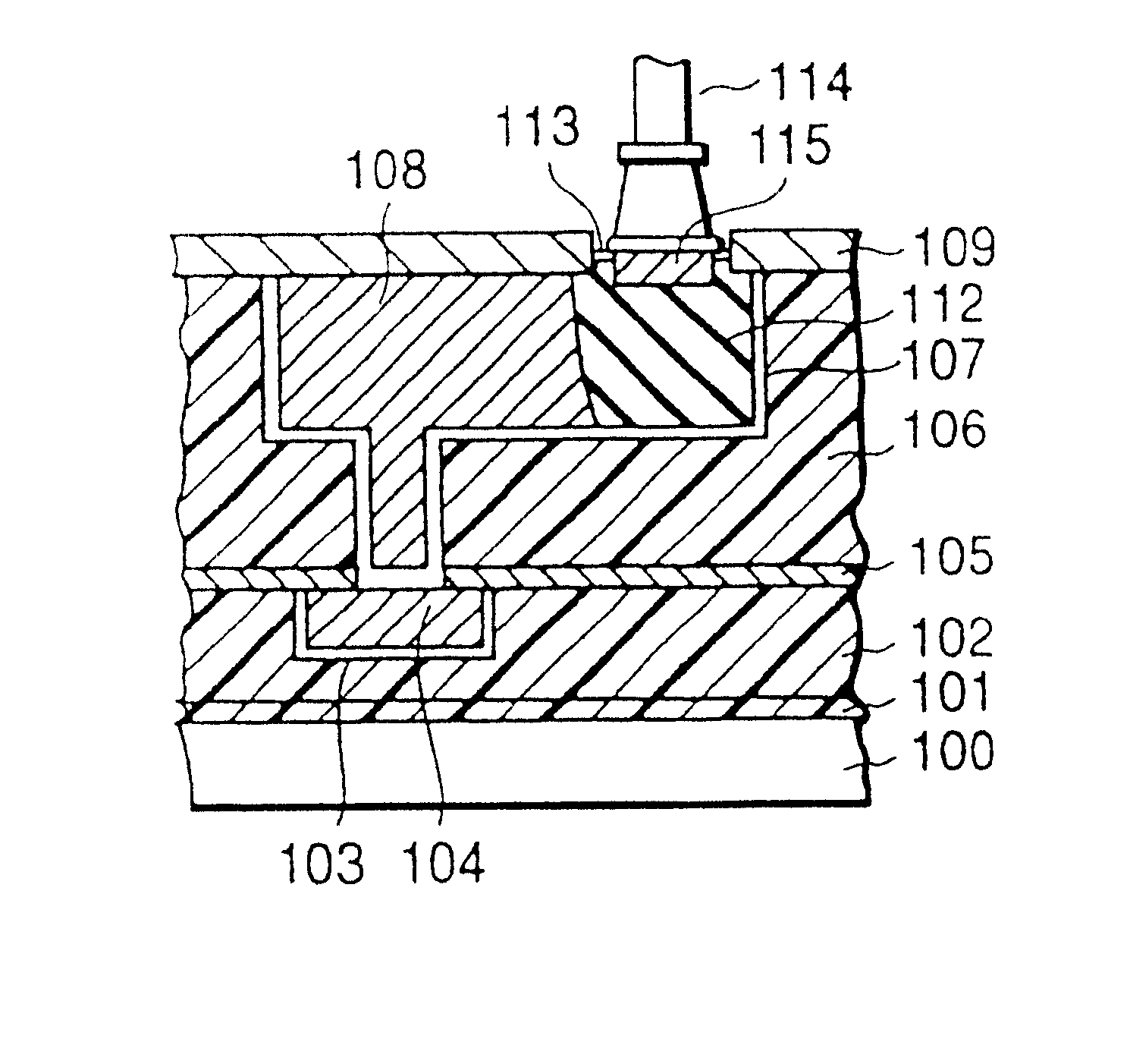
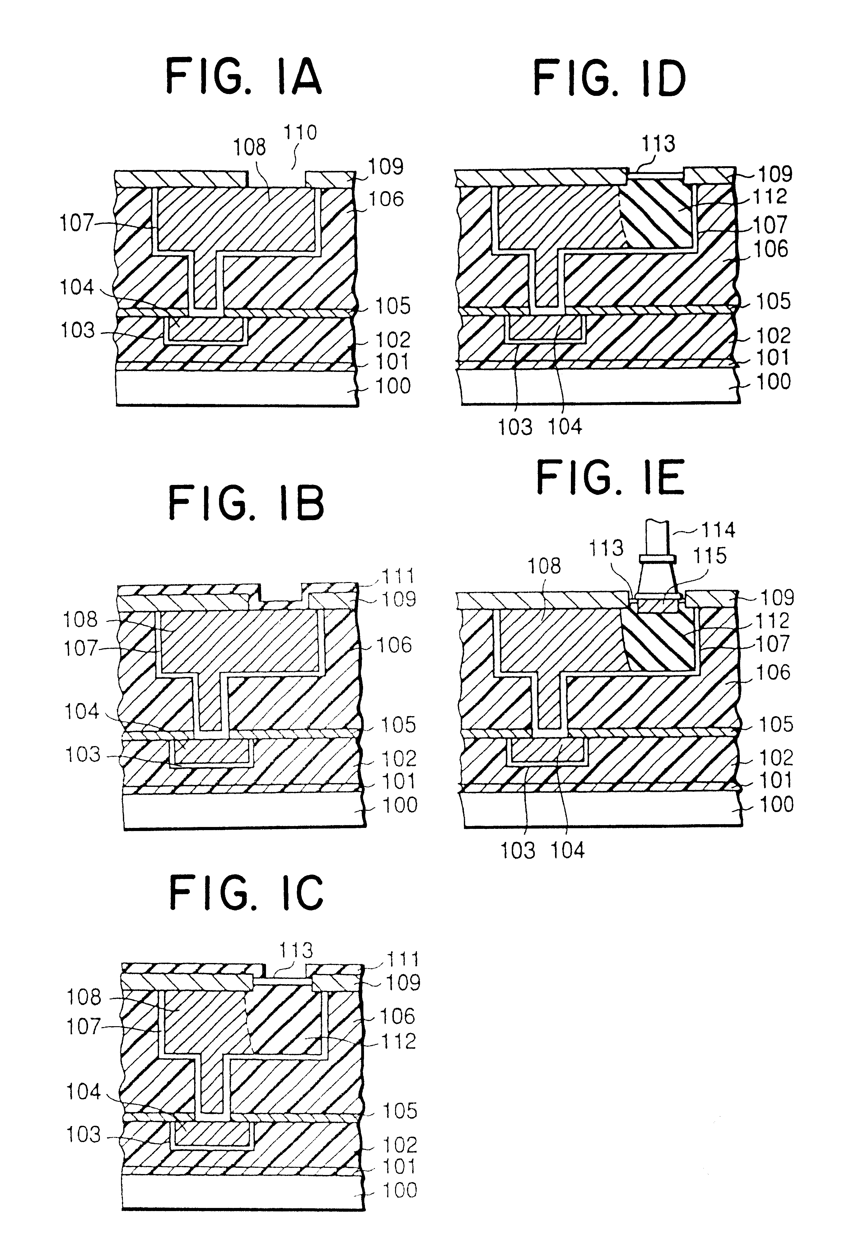
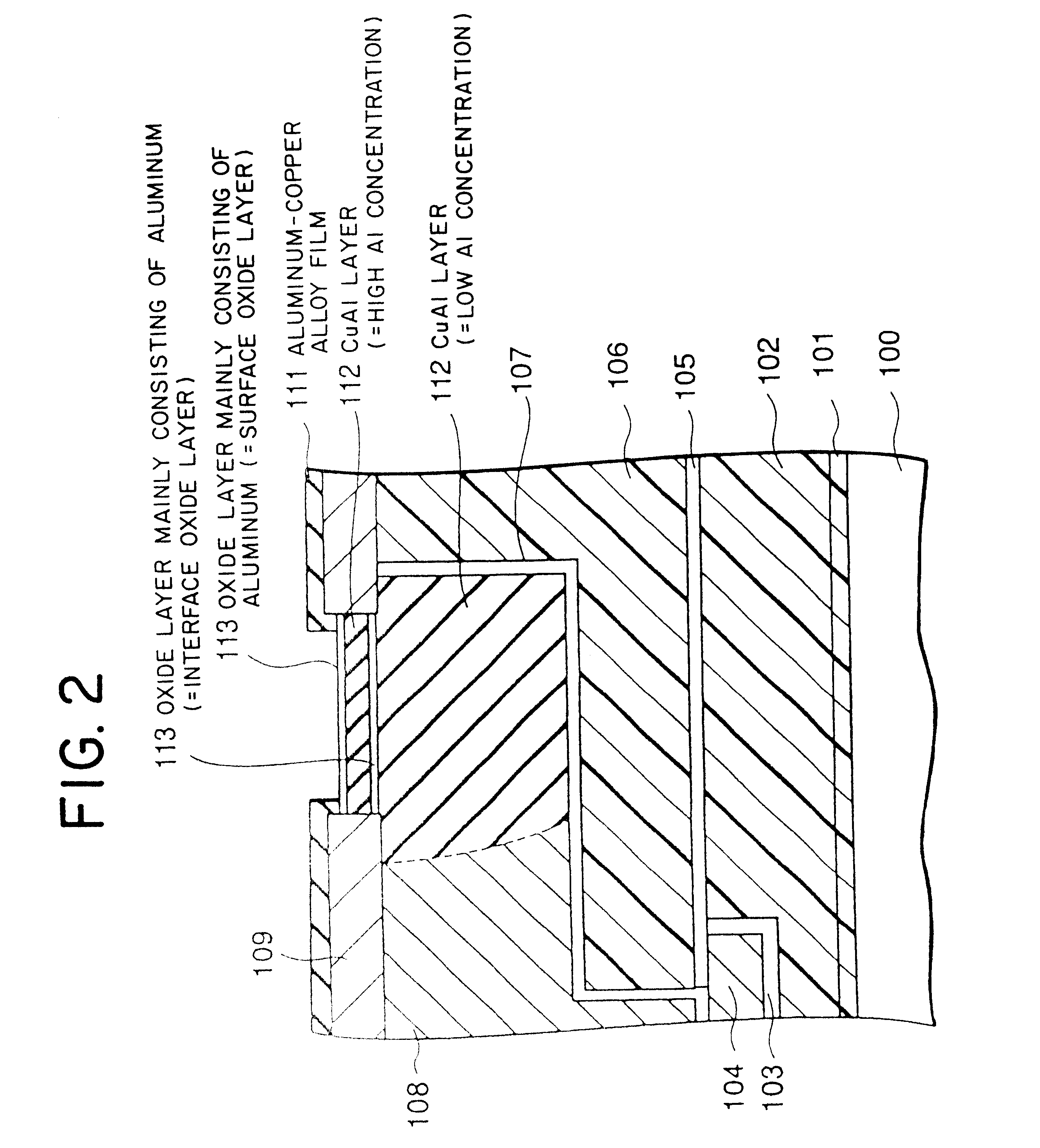
A first embodiment will be described with reference to FIG. 1A to FIG. 1E, FIG. 2, FIG. 3, and FIG. 4A to FIG. 4E.

In this embodiment, Cu is used as a material for the wiring layer, and aluminum (Al) is used as metal whose oxidation tendency is higher (easily oxidized) than Cu.

FIG. 1A to FIG. 1E show sectional diagrams of a direction in which wiring on the wiring layer, which is located on the top layer and has the pad electrode layer, extends.

First, a thermal oxidation silicon film (=SiO.sub.2 film) 101 is formed with a thickness of about 100 nm on a silicon (Si) substrate 100, and a silicon oxide film 102 is formed with a thickness of about 1 .mu.m by a CVD method.

Then, a so-called PEP process is performed by a lithography technology to form a pattern of a photoresist film on the silicon oxide film 102. The pattern is then used as a mask to perform dry etching to form a wiring pattern groove having a width of 1.3 .mu.m and a depth of 700 nm on the silicon oxide fi...

second embodiment

(Second Embodiment)

In this embodiment, Cu is used as a material for the wiring layer, and tantalum (Ta) is used as a metal whose oxidation tendency is higher (=easily oxidized) than Cu. Specifically, a tantalum (Ta) film is used in this embodiment instead of the AlCu film (or Al film) 111 used in the first embodiment.

The steps up to the formation of the opening in the SiN film (=insulating protective film) on the Cu wiring layer 108 described in the first embodiment (see FIG. 1A) can also be performed by the same procedure under the same conditions in this embodiment, so that the description about them is omitted. Therefore, like reference numerals are used for like component parts as those used in FIG. 1A to FIG. 1E of the first embodiment.

Now, this embodiment will be described with reference to FIG. 5A to FIG. 5C.

FIG. 5A to FIG. 5C show sectional diagrams showing a direction in which wiring is extended on the wiring layer having the pad electrode layer.

First, the SiN film 109 (=in...

third embodiment

(Third Embodiment)

In this embodiment, Cu is used as a material for the wiring layer, and titanium (Ti) is used as a metal whose oxidation tendency is higher (=readily oxidized) than Cu. Specifically, a titanium (Ti) film is used in this embodiment instead of the AlCu film (or Al film) 111, which is used in the first embodiment.

In this embodiment, the steps up to the formation of the opening in the SiN film 109 (=insulating protective film) on the Cu wiring layer 108 described in the first embodiment can be performed under the same condition by the same procedure, so that its description is omitted (See FIG. 1A). Therefore, like reference numerals are used to indicate like components as those shown in FIG. 1A to FIG. 1E of the first embodiment.

This embodiment will be described with reference to FIG. 6A to FIG. 6C.

FIG. 6A to FIG. 6C show sectional diagrams showing a direction in which wiring extends on the wiring layer which is on the top layer and has a pad electrode layer.

First, the...


PUM

PropertyMeasurementUnit
temperatureaaaaaaaaaa
thicknessaaaaaaaaaa

Abstract

A semiconductor device, which is comprised of a copper wiring layer which is formed above a semiconductor substrate, a pad electrode layer which conducts electrically to the copper wiring layer and has an alloy, which contains copper and a metal whose oxidation tendency is higher than copper, formed to extend to the bottom surface, and an insulating protective film which has an opening extended to the pad electrode layer, is provided.

Description

This application is based upon and claims the benefit of priority from the prior Japanese Patent Application No. 2001-57376 filed on Mar. 1, 2001, Japanese Patent Application No. 2001-260644 filed on Aug. 30, 2001, Japanese Patent Application No. 2001-401293 filed on Dec. 28, 2001 and Japanese Patent Application No. 2001-378778 filed on Dec. 12, 2001; the entire contents of which are incorporated herein by reference.1. Field of the InventionThe present invention relates to a semiconductor device and its manufacturing method, and more particularly to a semiconductor device with the reliability of connection by bonding or the like improved and its manufacturing method.2. Description of the Related ArtRecently, with the increase of the integration degree and operation velocity of the semiconductor device, copper (hereinafter called as "Cu") is used instead of aluminum (Al) or the like as a wiring material from the viewpoint of the reduction in resistance and high reliability of each wi...

Claims


Application Information

Patent Timeline
Patent Type & Authority Patents(United States)
IPC IPC(8): H01L21/60H01L21/70H01L21/02H01L23/532H01L23/485H01L21/768H01L23/52H01L23/48H01L21/28
CPCH01L21/76834H01L21/76846H01L21/76849H01L21/76858H01L21/76886H01L21/76888H01L23/53233H01L23/53238H01L24/03H01L24/05H01L24/11H01L24/48H01L22/32H01L23/53295H01L24/45H01L2224/02166H01L2224/04042H01L2224/05009H01L2224/05082H01L2224/05083H01L2224/05093H01L2224/05147H01L2224/05166H01L2224/05181H01L2224/05187H01L2224/05546H01L2224/05558H01L2224/05567H01L2224/05605H01L2224/05611H01L2224/05613H01L2224/05616H01L2224/0562H01L2224/05624H01L2224/05639H01L2224/05644H01L2224/05647H01L2224/13099H01L2224/13105H01L2224/13109H01L2224/13111H01L2224/13113H01L2224/13116H01L2224/1312H01L2224/13124H01L2224/13139H01L2224/13144H01L2224/45105H01L2224/45109H01L2224/45111H01L2224/45113H01L2224/45116H01L2224/4512H01L2224/45124H01L2224/45139H01L2224/45144H01L2224/4807H01L2224/48463H01L2224/48505H01L2224/48624H01L2224/48647H01L2224/48724H01L2224/48747H01L2224/85375H01L2924/01004H01L2924/01006H01L2924/01007H01L2924/01012H01L2924/01013H01L2924/01014H01L2924/01015H01L2924/01022H01L2924/01027H01L2924/01028H01L2924/01029H01L2924/01031H01L2924/01033H01L2924/0104H01L2924/01042H01L2924/01047H01L2924/01049H01L2924/0105H01L2924/01051H01L2924/01073H01L2924/01074H01L2924/01078H01L2924/01079H01L2924/01082H01L2924/01083H01L2924/01327H01L2924/04953H01L2924/05042H01L2924/01019H01L2924/01023H01L2924/01024H01L2924/01041H01L2924/01044H01L2924/01072H01L2224/05557H01L2224/05559H01L2224/45147H01L2224/48453H01L2224/48644H01L2224/48611H01L2224/48616H01L2224/48639H01L2224/48711H01L2224/48739H01L2224/48716H01L2224/48799H01L2924/10253H01L2224/05552H01L2224/0401H01L2924/0002H01L2924/00014H01L2924/04941H01L2224/05609H01L2924/00H01L2224/48744H01L2224/48713H01L2224/48705H01L2224/4872H01L2224/48605H01L2224/48613H01L2224/4862H01L2224/48811H01L2224/48824H01L2224/48839H01L2224/48844H01L2224/48847H01L2224/48805H01L2224/48813H01L2224/48816H01L2224/4882H01L2924/12042H01L2224/05017H01L2224/0392H01L2224/03921H01L2924/00015H01L2224/45015H01L2924/207H01L21/28
Inventor TOYODA, HIROSHINAKAO, MITSUHIROHASUNUMA, MASAHIKOKANEKO, HISASHISAKATA, ATSUKOKOMUKAI, TOSHIAKI
Owner KIOXIA CORP
Learn More