

Semiconductor device and manufacturing method of semiconductor device
a semiconductor and semiconductor technology, applied in the field of semiconductor devices, can solve the problems of long processing time, defective bonded parts, and inability to perform bonding steps
- Summary
- Abstract
- Description
- Claims
- Application Information
AI Technical Summary
Benefits of technology
Problems solved by technology
Method used
Image

Examples
first embodiment
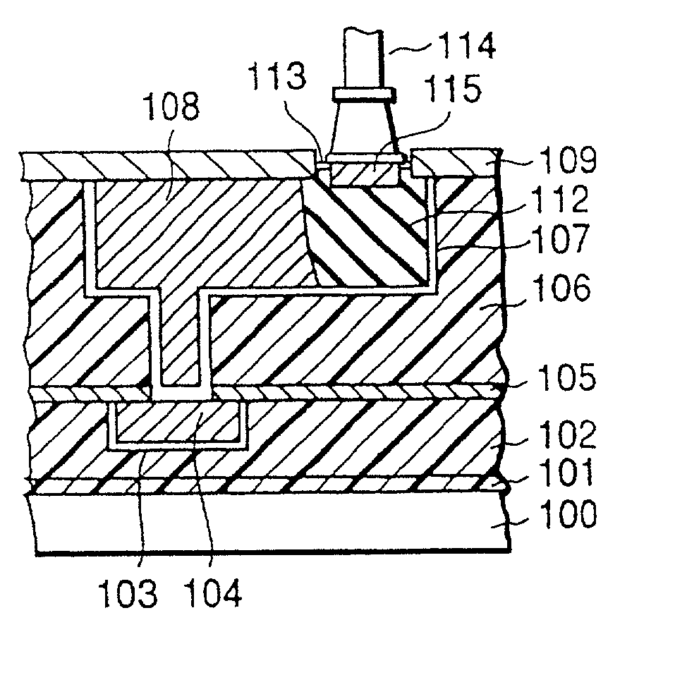
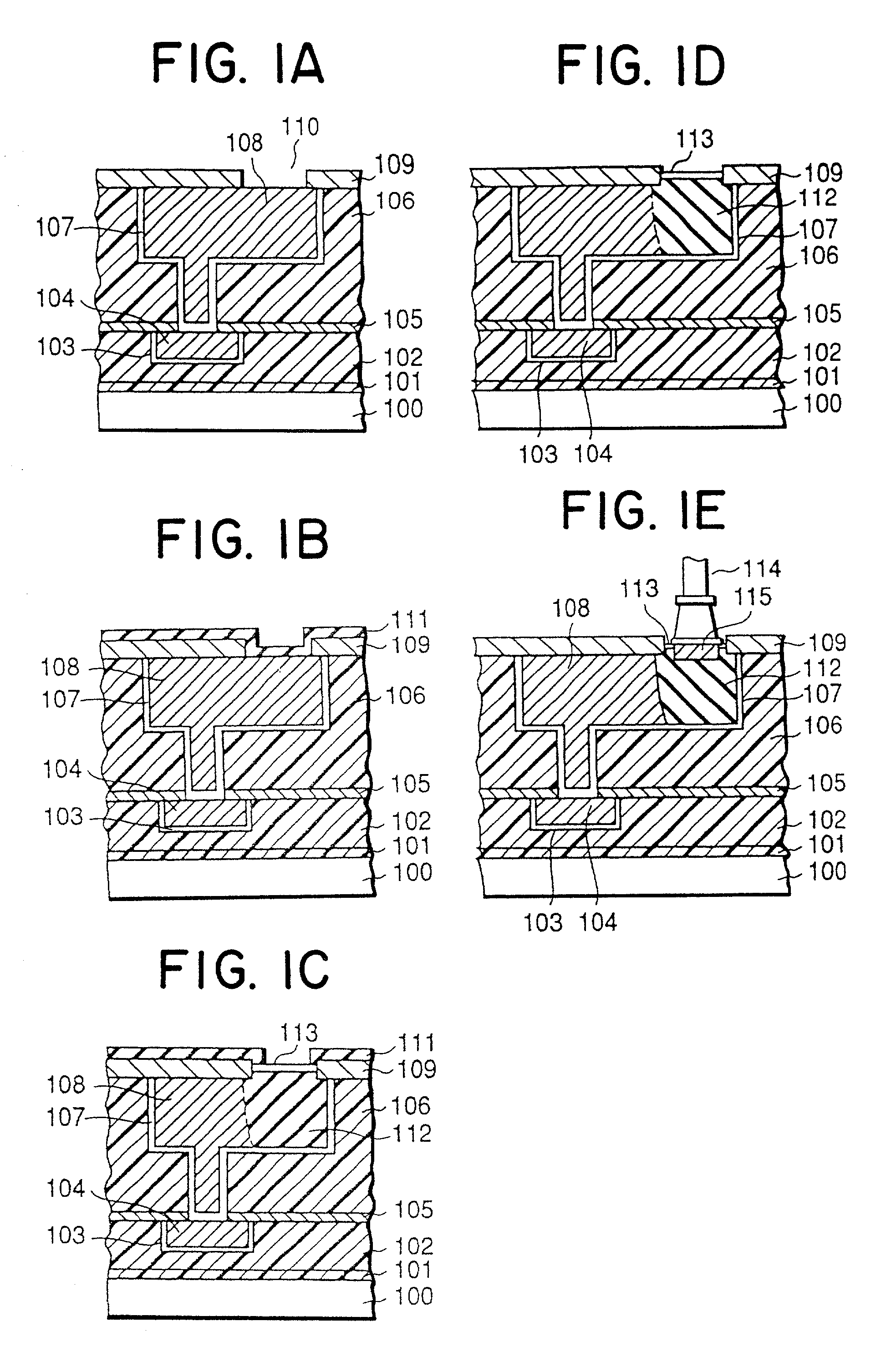
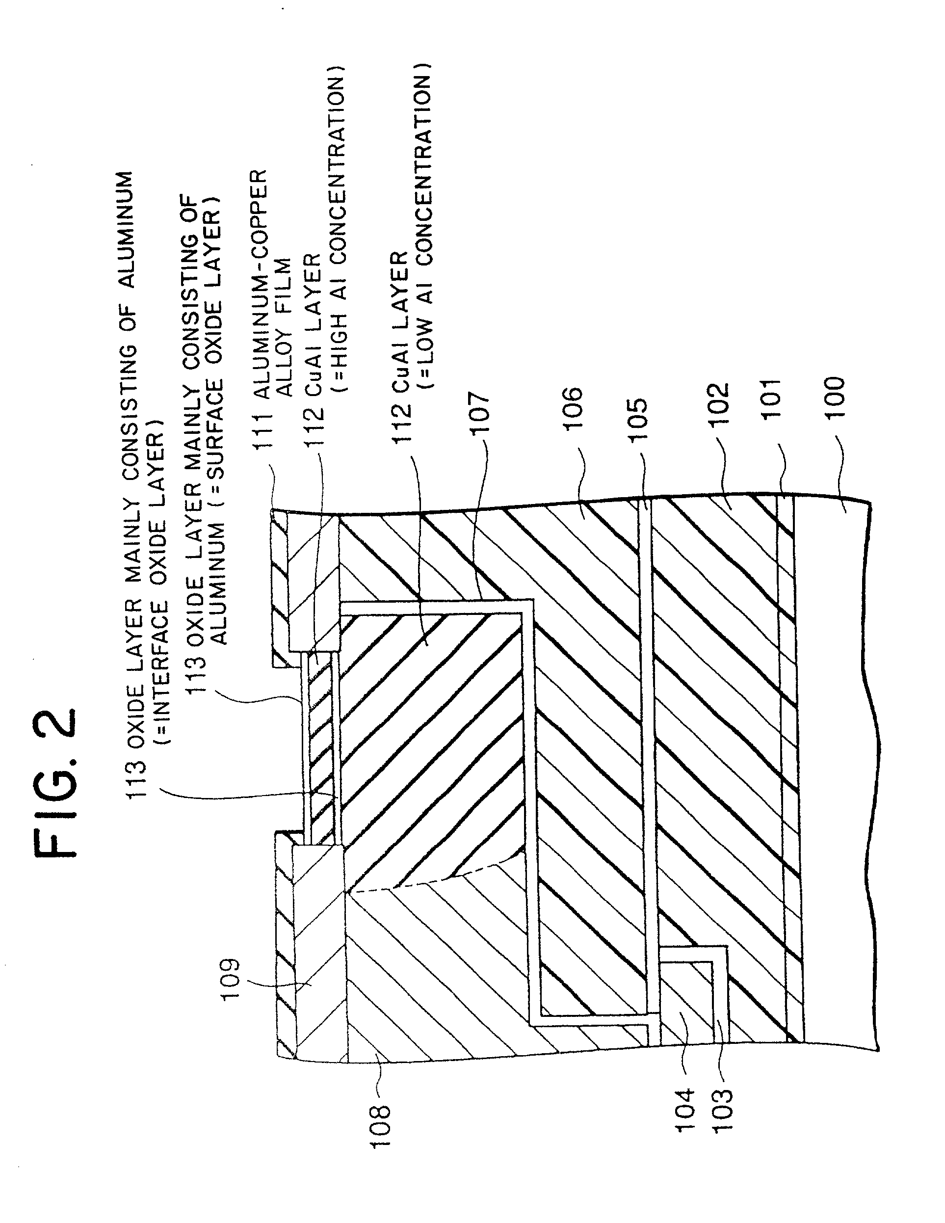
[0114] (First Embodiment)
[0115] A first embodiment will be described with reference to FIG. 1A to FIG. 1E, FIG. 2, FIG. 3, and FIG. 4A to FIG. 4E.
[0116] In this embodiment, Cu is used as a material for the wiring layer, and aluminum (Al) is used as metal whose oxidation tendency is higher (easily oxidized) than Cu.
[0117] FIG. 1A to FIG. 1E show sectional diagrams of a direction in which wiring on the wiring layer, which is located on the top layer and has the pad electrode layer, extends.
[0118] First, a thermal oxidation silicon film (=SiO.sub.2 film) 101 is formed with a thickness of about 100 nm on a silicon (Si) substrate 100, and a silicon oxide film 102 is formed with a thickness of about 1 .mu.m by a CVD method.
[0119] Then, a so-called PEP process is performed by a lithography technology to form a pattern of a photoresist film on the silicon oxide film 102. The pattern is then used as a mask to perform dry etching to form a wiring pattern groove having a width of 1.3 .mu.m and...
second embodiment
[0183] (Second Embodiment)
[0184] In this embodiment, Cu is used as a material for the wiring layer, and tantalum (Ta) is used as a metal whose oxidation tendency is higher (=easily oxidized) than Cu. Specifically, a tantalum (Ta) film is used in this embodiment instead of the AlCu film (or Al film) 111 used in the first embodiment.
[0185] The steps up to the formation of the opening in the SiN film (=insulating protective film) on the Cu wiring layer 108 described in the first embodiment (see FIG. 1A) can also be performed by the same procedure under the same conditions in this embodiment, so that the description about them is omitted. Therefore, like reference numerals are used for like component parts as those used in FIG. 1A to FIG. 1E of the first embodiment.
[0186] Now, this embodiment will be described with reference to FIG. 5A to FIG. 5C.
[0187] FIG. 5A to FIG. 5C show sectional diagrams showing a direction in which wiring is extended on the wiring layer having the pad electrode...
third embodiment
[0208] (Third Embodiment)
[0209] In this embodiment,Cu is used as a material for the wiring layer, and titanium (Ti) is used as a metal whose oxidation tendency is higher (=readily oxidized) than Cu. Specifically, a titanium (Ti) film is used in this embodiment instead of the AlCu film (or Al film) 111, which is used in the first embodiment.
[0210] In this embodiment, the steps up to the formation of the opening in the SiN film 109 (=insulating protective film) on the Cu wiring layer 108 described in the first embodiment can be performed under the same condition by the same procedure, so that its description is omitted (See FIG. 1A). Therefore, like reference numerals are used to indicate like components as those shown in FIG. 1A to FIG. 1E of the first embodiment.
[0211] This embodiment will be described with reference to FIG. 6A to FIG. 6C.
[0212] FIG. 6A to FIG. 6C show sectional diagrams showing a direction in which wiring extends on the wiring layer which is on the top layer and ha...
PUM
| Property | Measurement | Unit |
|---|---|---|
| diameter | aaaaa | aaaaa |
| length | aaaaa | aaaaa |
| thickness | aaaaa | aaaaa |
Abstract
Description
Claims
Application Information