Method and device for fabricating a layer in semiconductor material

a technology of semiconductor material and substrate, which is applied in the direction of polycrystalline material growth, crystal growth process, chemistry apparatus and processes, etc., can solve the problems of inability to obtain substrates in single-crystalline materials, method not adapted to obtain substrates, and ingot pulling using the czochralsky process

Inactive Publication Date: 2016-12-27
SOITEC SA
View PDF90 Cites 0 Cited by
  • Summary
  • Abstract
  • Description
  • Claims
  • Application Information

AI Technical Summary

Benefits of technology

[0019]It is one objective of the invention to produce semiconductor substrates, both of narrow thickness (e.g., 50 microns) and of larger thickness (e.g., from 500 to 1000 microns), and having large lateral dimensions (e.g., a diameter of 300 mm or even larger) by avoiding or limiting the afore-mentioned shortcomings.
[0034]the dynamics of the movement of the substrate toward the liquid surface is controlled to minimize the time spent by the substrate at a very short distance (less than 1 mm) from the liquid surface,
[0066]The arm system allowing rapidly bringing the main jack system and the fine actuators and thus the substrate to above the liquid surface at a well-calibrated distance, for example, of a few mm,
[0068]The system of “fine” actuators allowing the angle of the surface of the donor substrate to be varied and thus allowing an adjustment of the orientation of the substrate with respect to the liquid surface.

Problems solved by technology

With this method, it is not possible to obtain substrates in single-crystalline material, although it is generally desired to have single-crystalline material for microelectronic applications.
Additionally, this method is not adapted for obtaining a substrate from a donor substrate in which a weakened zone has been fainted.
Ingot pulling using the Czochralsky process may give rise to problems, in particular if the ingot is of large diameter (e.g., 300 mm or 450 mm).
When it is desired to increase the diameter of the ingot and hence of the substrates derived therefrom, the extraction of the latent heat from solidification of the ingot becomes increasingly more difficult.
In addition, it is likely to create non-homogeneities inside the ingot.
These cutting and treating operations are relatively costly.
In addition, they have the disadvantage of consuming a significant part of the ingot mass, and they can only lead with difficulty—even not at all—to the obtaining of thin substrates.
For example, by sawing an ingot, it is not possible to obtain thin substrates having a thickness of 50 microns, for example.
Limitations of this type of method follow from the slowness of the process and its cost.

Method used


Image

  • Method and device for fabricating a layer in semiconductor material
  • Method and device for fabricating a layer in semiconductor material
  • Method and device for fabricating a layer in semiconductor material

Examples


examples

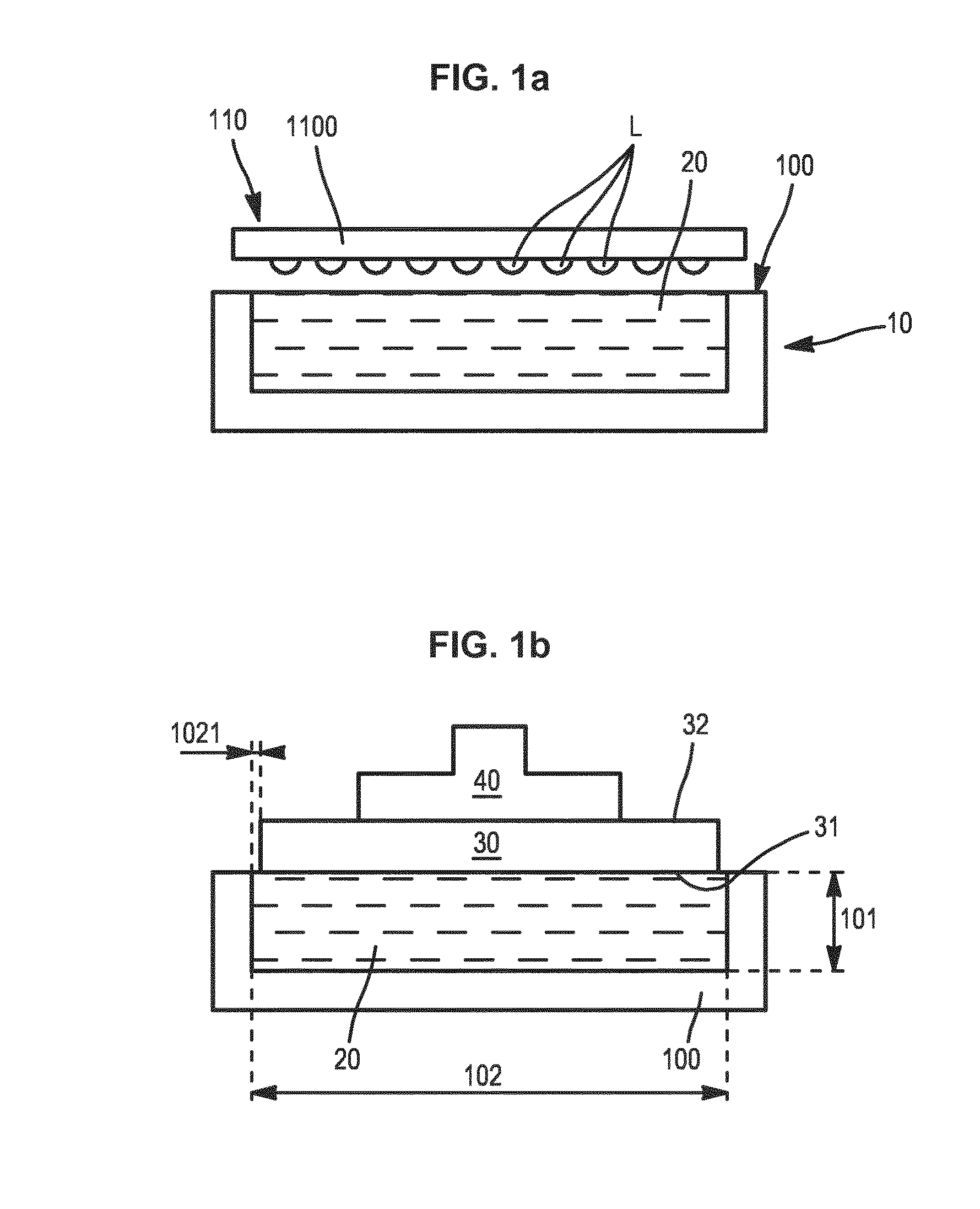
[0379]As an example, the method can be carried out and a good quality layer can be solidified with the following parameters:[0380]donor substrate material: Si[0381]bath material: Si[0382]Diameter of the donor substrate (disc shape) and of the bath: 300 mm[0383]initial thickness of the donor substrate: 900 microns[0384]bath depth: 100 microns[0385]implantation depth (e0): 2-4 microns (two different values were considered).

[0386]According to another example, the following parameters can be chosen:[0387]donor substrate material: Ge[0388]bath material: Ge[0389]initial thickness of the donor substrate: 400 microns[0390]Diameter 150 mm (disc shape)[0391]bath depth: 150 microns[0392]implantation depth (e0): 1 to 2 microns (two different values were considered).

[0393]According to another example the following parameters can be chosen:[0394]Si materials for the donor substrate[0395]material (Si 0.9-Ge 0.1) for the liquid phase[0396]initial thickness of the donor substrate: 900 microns[0397]D...


PUM

PropertyMeasurementUnit
distancesaaaaaaaaaa
diameteraaaaaaaaaa
diameteraaaaaaaaaa

Abstract

The invention concerns a method for fabricating a substrate in semiconductor material characterized in that it comprises the steps of: starting from a donor substrate in a first semiconductor material at an initial temperature, contacting a surface of the donor substrate with a bath of a second semiconductor material held in the liquid state at a temperature higher than the initial temperature, the second semiconductor material being chosen so that its melting point is equal to or lower than the melting point of the first semiconductor material, solidifying the bath material on the surface to thicken the donor substrate with a solidified layer. The invention also concerns a device for implementing the method.

Description

CROSS-REFERENCE TO RELATED APPLICATIONS[0001]This application is a national phase entry under 35 U.S.C. §371 of International Patent Application PCT / EP2012 / 064633, filed Jul. 25, 2012, designating the United States of America and published in English as International Patent Publication WO 2013 / 014209 A1 on Jan. 31, 2013, which claims the benefit under Article 8 of the Patent Cooperation Treaty and under 35 U.S.C. §119(e) to French Patent Application Ser No. 1156770 filed Jul. 25, 2011, the disclosure of each of which is hereby incorporated herein in its entirety by this reference.FIELD OF THE INVENTION[0002]The present invention concerns a method for fabricating substrates in semiconductor material. The invention also applies to the fabrication of substrates in silicon, germanium or silicon-germanium compounds, this list not being limiting.[0003]The invention further concerns a device for fabricating semiconductor substrates.BACKGROUND OF THE INVENTION[0004]Different methods exist f...

Claims


Application Information

Patent Timeline
Patent Type & Authority Patents(United States)
IPC IPC(8): C30B11/14C30B19/00C30B29/08C30B19/06H01L21/02C30B19/10C30B29/06
CPCC30B19/10C30B19/00C30B19/062C30B29/06C30B29/08H01L21/02532H01L21/02625
Inventor BRUEL, MICHEL
Owner SOITEC SA
Why Eureka
Try Eureka