Standard cell library with DFM-optimized M0 cuts

Active Publication Date: 2016-12-27
PDF SOLUTIONS INC
View PDF4 Cites 5 Cited by
  • Summary
  • Abstract
  • Description
  • Claims
  • Application Information

AI Technical Summary

Benefits of technology

[0007]Applicant has discovered that, with very careful design, seemingly incompatible demands for cell density and avoidance of certain difficult-to-manufacture features can be simultaneously achieved. In particular, as exemplified by the depicted cells herein, the present

Problems solved by technology

As semiconductor processes advance to render increasingly smaller features, the des

Method used


Image

  • Standard cell library with DFM-optimized M0 cuts
  • Standard cell library with DFM-optimized M0 cuts
  • Standard cell library with DFM-optimized M0 cuts

Examples


Example

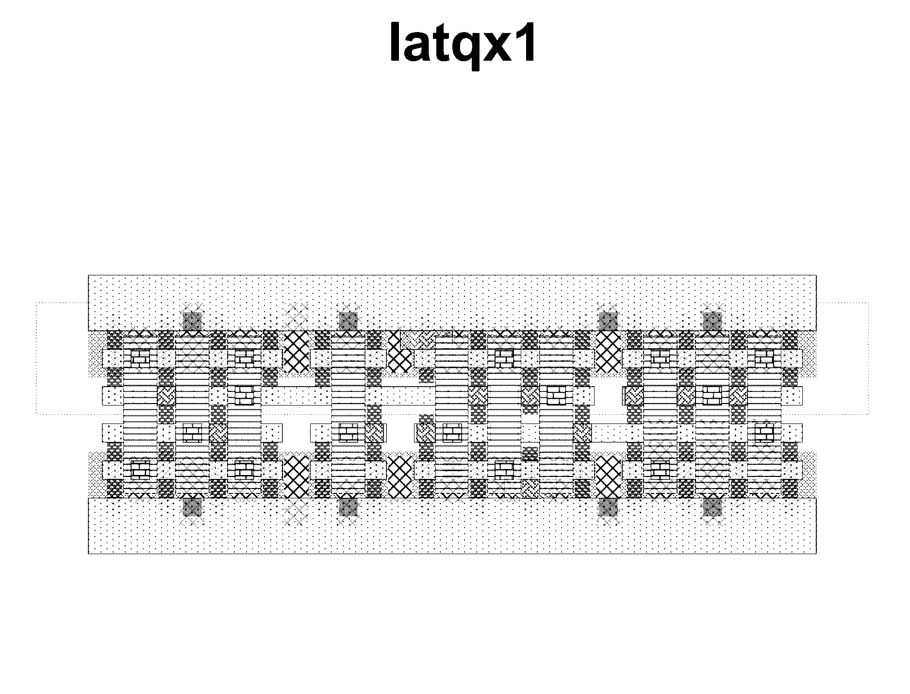
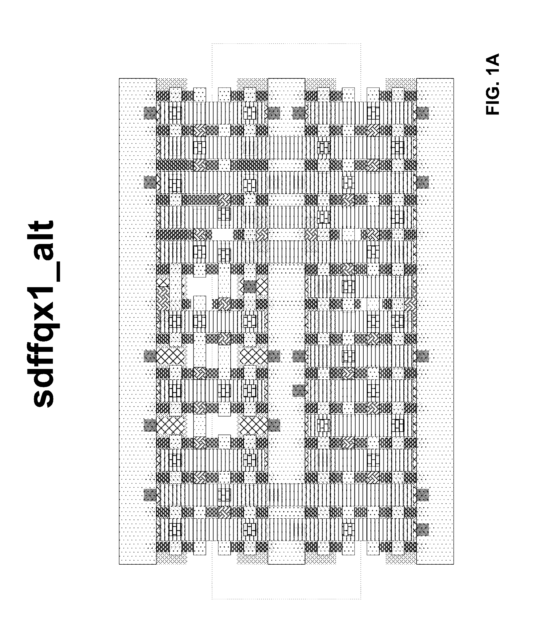
[0155]FIGS. 92-94 show layer maps for the respective A-labeled, B-labeled and C-labeled figures that follow. With reference to FIG. 92, the full set of depicted layers includes: M0 (first metal), NW (N-well), TS (trench silicide), RX (active), CA (contact to active), PC (gate, a / k / a polysilicon or poly—although the gate material in advanced processes is typically metallic), GO (gate open, a / k / a CB), V0 (via to interconnect), and M1 (first-level interconnect). Persons skilled in the art will appreciate that any of these layers may be created through multiple exposure (e.g., double, triple or quadruple patterned) processes, and / or through use of cut masks, which themselves may be multi-patterned. The A-labeled figures in this application are intended to show the resulting complete cells as clearly as possible; thus, the details of multi-patterning and cut-masking have been eliminated from these figures.

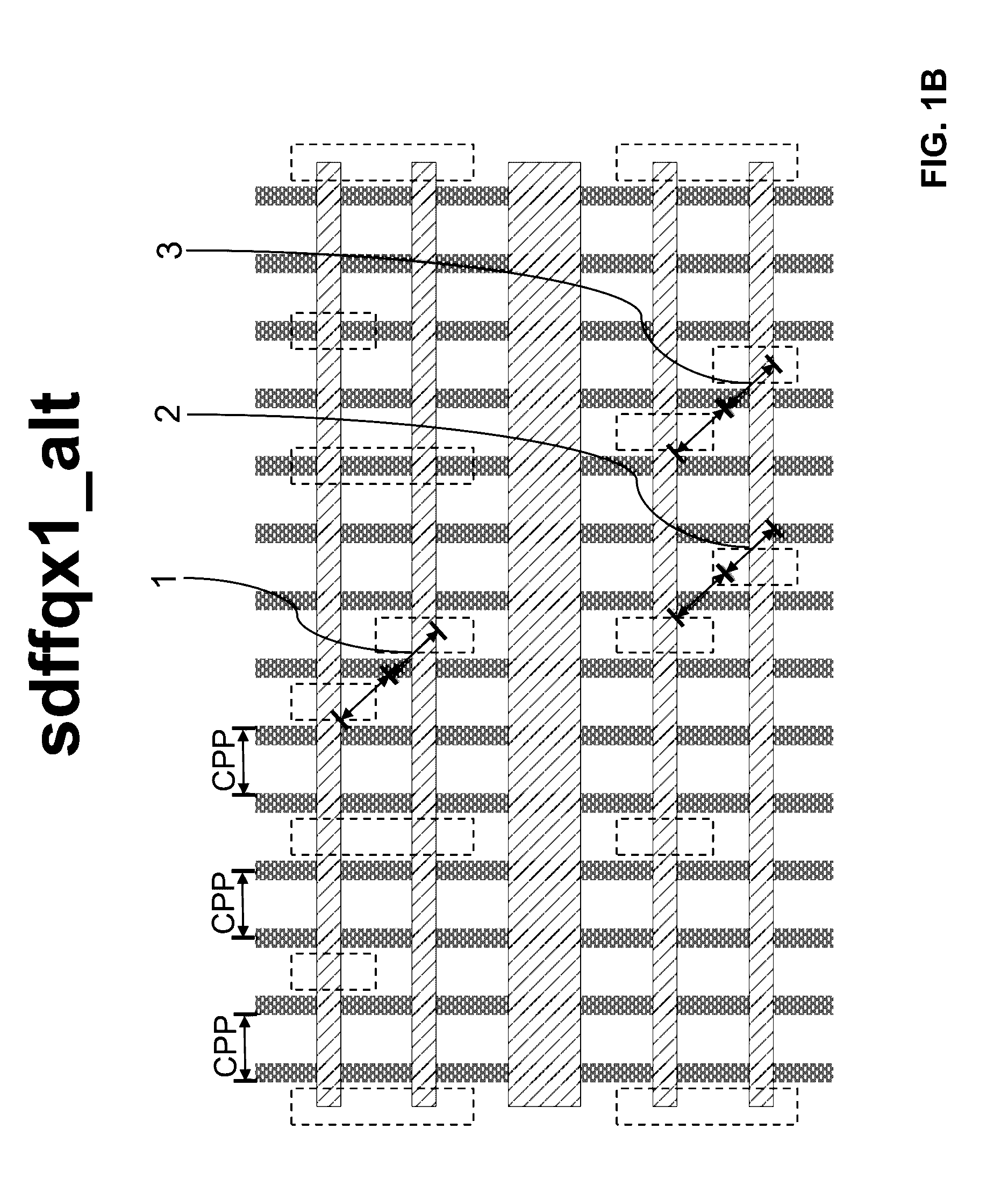
[0156]Referring now to FIGs. 93 and 94, these show the layer maps for the B-labeled...


PUM


Abstract

A library of a DFM-improved standard logic cells that avoid pattern-degrading configurations in the M0 layer is disclosed, along with wafers, chips and systems constructed from such cells.

Description

[0001]A portion of the disclosure of this patent document contains material which is subject to mask work protection, *M*, PDF Solutions, Inc. The mask work owner (PDF Solutions, Inc.) has no objection to the facsimile reproduction by anyone of the patent document or the patent disclosure, as it appears in the Patent and Trademark Office patent file or records, but otherwise reserves all mask work rights whatsoever.FIELD OF THE INVENTION[0002]This invention relates to design for manufacturability (DFM) of standard cells for advanced semiconductor processes (e.g., 10 nm, 7 nm), to libraries containing such cells, and to wafers / chips that contain instances of such cells.BACKGROUND OF THE INVENTION[0003]As semiconductor processes advance to render increasingly smaller features, the design of dense, high-yielding (manufacturable) cells becomes increasingly challenging. See, e.g., U.S. Pat. No. 9,202,820, “Flip-flop, latch, and mux cells for use in a standard cell library and integrated ...

Claims


Application Information

Patent Timeline
IPC IPC(8): G06F17/50H01L27/118H01L27/02
CPCG06F17/5068H01L27/11807H01L27/0207H01L2027/11883H01L2027/11885G06F30/39
Inventor HAIGH, JONATHAN
Owner PDF SOLUTIONS INC
Why Eureka
Try Eureka