High-order polarization conversion device, optical waveguide device, and DP-QPSK modulator
a conversion device and high-order technology, applied in the direction of instruments, optical waveguide light guides, optical light guides, etc., can solve the problems of increasing the size and cost of the device, the structure of the optical circuit components that form the optical modulator is complicated, and it is difficult to perform the optical modulation operation. , to achieve the effect of different widths
- Summary
- Abstract
- Description
- Claims
- Application Information
AI Technical Summary
Benefits of technology
Problems solved by technology
Method used
Image
Examples
example 1
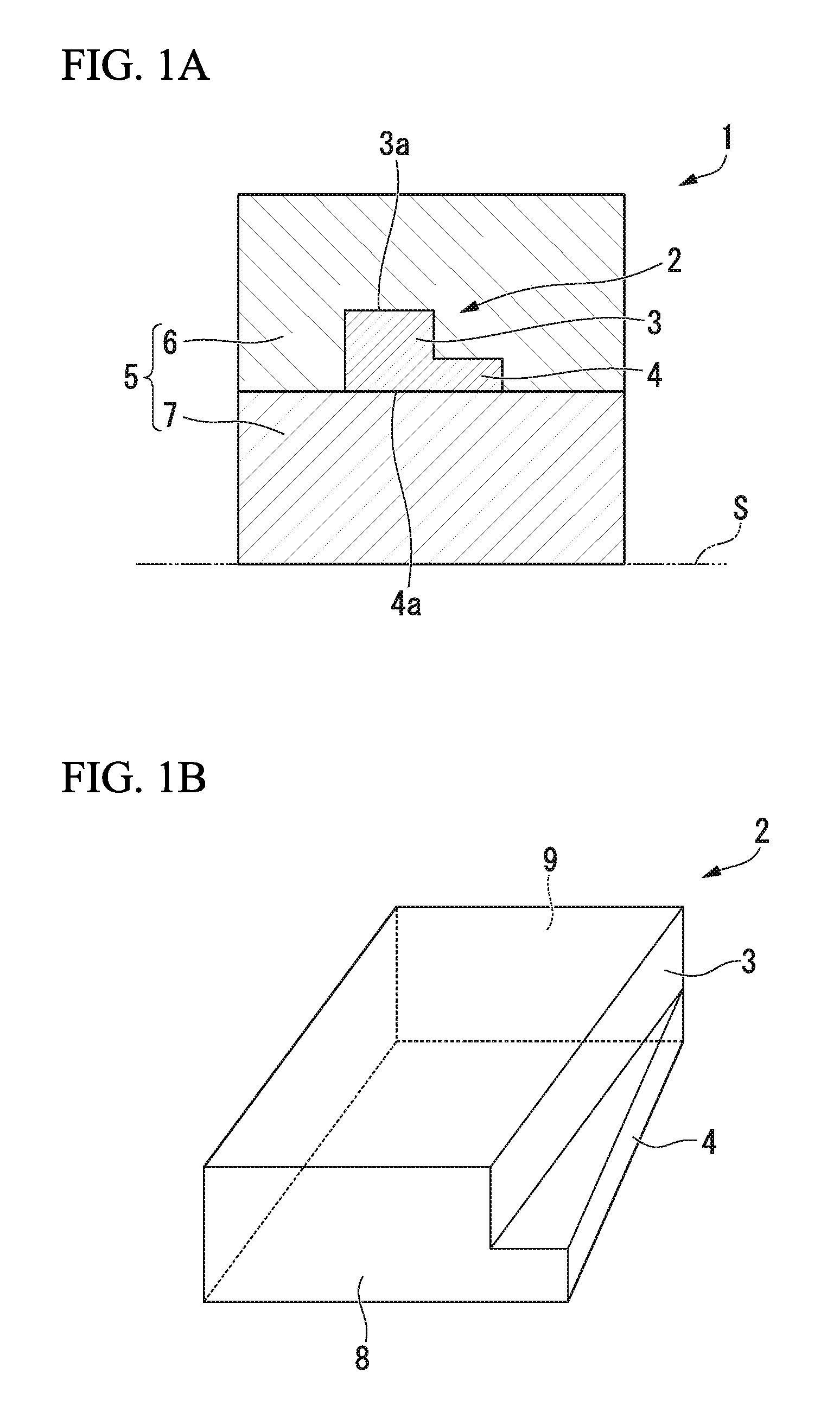
[0247]Based on Calculation Example 1, a waveguide device of Example 1 having a structure (refer to the first embodiment described above) in which the upper core is located at the center of the lower core is manufactured.
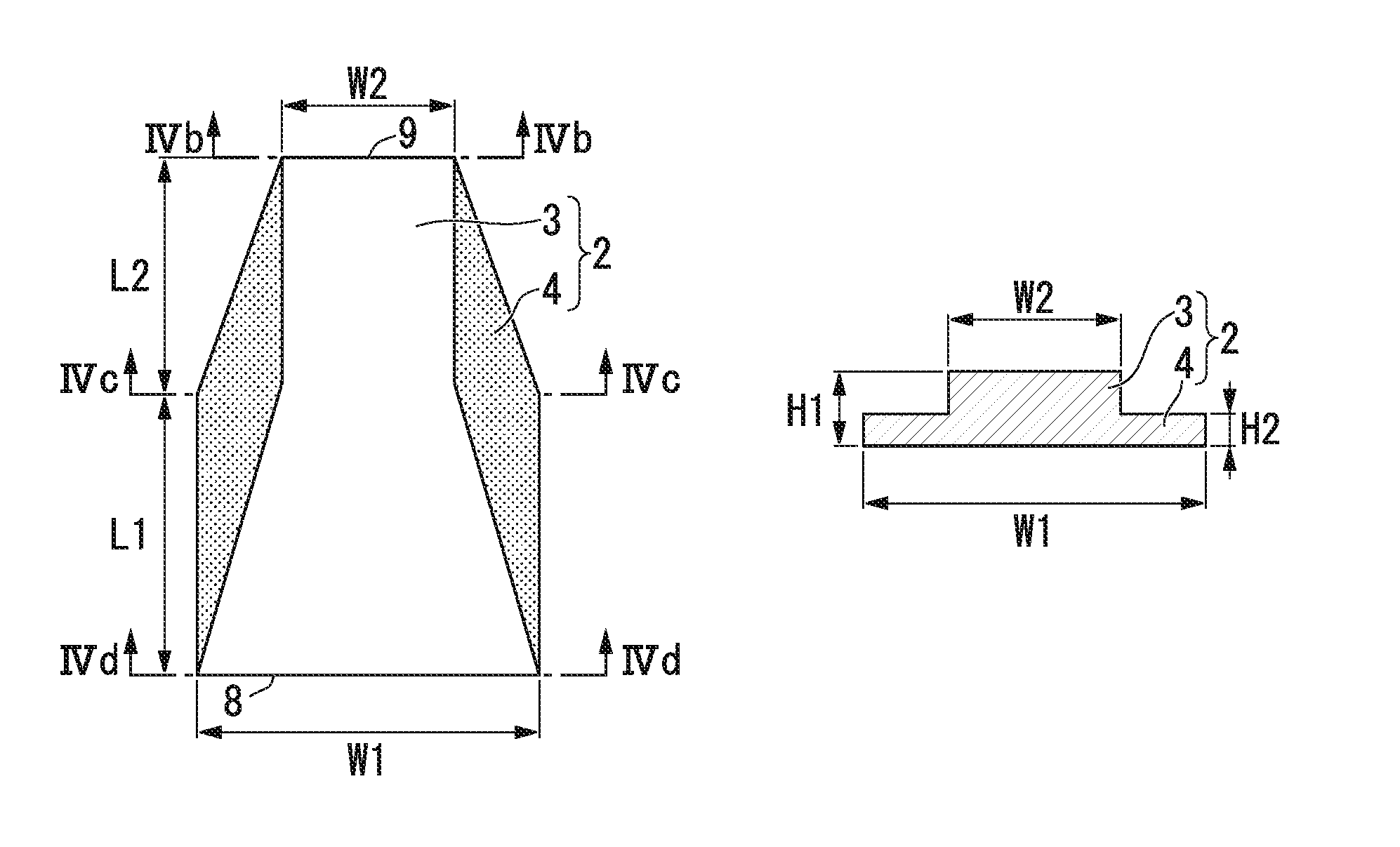
[0248]FIGS. 4A to 4D are diagrams showing the device of this example. In this example, a waveguide is manufactured based on a silicon on insulator (SOI) substrate formed of Si—SiO2—Si. An intermediate SiO2 layer is used as a lower clad, and an upper Si layer is used as a core. After forming the core, the SiO2 layer is disposed as an upper clad.
[0249]The height H2 of the lower core 4 is 0.095 μm, the height (difference of H1-H2) of the upper core 3 is 0.125 μm, and the core height H1 including the lower core 4 and the upper core 3 is 0.22 μm. At the start portion 8, the width W1 of each of the upper core and the lower core is 0.84 μm. In a section L2 (15 μm in length), the width W2 of the upper core 3 is 0.5 μm, and the upper core 3 is located at the center of the low...
example 2
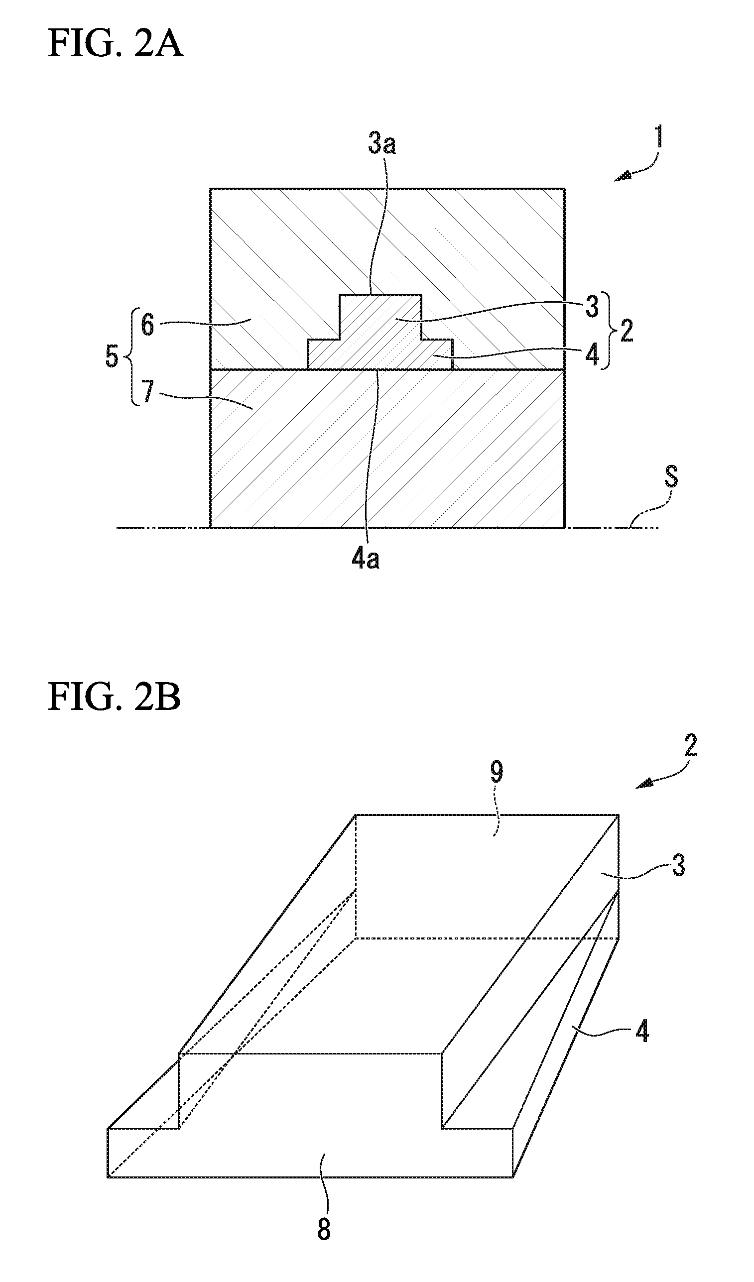
[0258]As shown in FIGS. 5A to 5D, a high-order polarization conversion device having a structure in which ends of the upper core and the lower core match each other (refer to the second embodiment described above) is manufactured using the same method as in Example 1.
[0259]The height H2 of the lower core 4 is 0.095 μm, the height (difference of H1−H2) of the upper core 3 is 0.125 μm, and the core height H1 including the lower core 4 and the upper core 3 is 0.22 μm. At the start portion 8, the width W1 of each of the upper core and the lower core is 0.84 μm. In a section L2 (15 μm in length), the width W2 of the upper core 3 is 0.5 μm. In a section L1 (20 μm in length), the width W1 of the lower core 4 is 0.84 μm. In addition, over the entire length of the sections L1 and L2, the upper core and the lower core are located so that the ends of the upper core and the lower core match each other. At the end portion 9, the width W2 of each of the upper core and the lower core is 0.5 μm.
[02...
example 3
[0261]As shown in FIGS. 6A to 6C, a high-order polarization conversion device having a structure (refer to the third embodiment described above) in which the sectional shape of the start portion 8 is a rib waveguide, the sectional shape of the end portion 9 is a rectangular waveguide, and the centers of the upper core 3 and the lower core 4 in the width direction match each other.
[0262]The height H2 of the lower core 4 is 0.095 μm, the height (difference of H1-H2) of the upper core 3 is 0.125 μm, and the core height H1 including the lower core 4 and the upper core 3 is 0.22 μm. At the start portion 8, the width W1a of the upper core 3 is 1 μm, and the width W1 of the lower core 4 is 4 μm. At the end portion 9, the width W2 of each of the upper core and the lower core is 0.5 μm. The maximum core width of the start portion 8 is 4 μm that is limited, but the distribution of TE1 passing through the section is sufficiently inward from both ends of the lower core 4 of the start portion 8....
PUM
 Abstract
Description
Claims
Application Information


