Damascene method of forming a semiconductor structure and a semiconductor structure with multiple fin-shaped channel regions having different widths

a technology of fin-shaped channel region and semiconductor structure, which is applied in the direction of semiconductor devices, electrical devices, basic electric elements, etc., can solve the problems of limited performance of tuning devices in this manner, increased risk of damage, and fin damag

Inactive Publication Date: 2012-05-03
GLOBALFOUNDRIES INC
View PDF0 Cites 9 Cited by
  • Summary
  • Abstract
  • Description
  • Claims
  • Application Information

AI Technical Summary

Benefits of technology

[0018]An embodiment of a semiconductor structure formed according to this method embodiment can comprise a first semiconductor region for a first non-planar multi-gate field effect transistor (MUGFET) and a second semiconductor region, positioned laterally adjacent to the first semiconductor region, for a second MUGFET. The first semiconductor region and the second semiconductor region can be defined by a trench isolation structure. That is, a trench isolation structure on the insulator layer can laterally surround the first semiconductor region and the second semiconductor region such that the first semiconductor region is electrically isolated from the second semiconductor region. The first semiconductor region can have first end portions and a first center portion positioned laterally between the first end portions. The first center portion can be narrower than the first end portions (e.g., can be essentially fin-shaped) and can have a first width. Optionally, a first isolating cap can be positioned on the first center portion and can have the same first width. The first isolating cap can comprise a dielectric body positioned laterally between dielectric spacers. The second semiconductor region can have second end portions and a second center portion positioned laterally between the second end portions. The second center portion can be narrower than the second end portions and can comprise two parallel sections. Each of these parallel sections can be essentially fin-shaped and can have a second width that is less than the first width. Optionally, second isolating caps can be positioned on the parallel sections and can have the same second width. Each second isolating cap can be essentially identical to one of the dielectric spacers of the first isolating cap.

Problems solved by technology

Unfortunately, tuning device performance in this manner is limited by current MUGFET processing techniques.
For example, if one or more relatively thin semiconductor fins are formed for a dual-gate or tri-gate FET and then one or more dopant implantation processes (e.g., source / drain extension implantation, halo implantation, source / drain implantation, etc.) are performed, fin damage can occur.
The risk of damage increases significantly as the fin width within the channel region decreases.

Method used


Image

  • Damascene method of forming a semiconductor structure and a semiconductor structure with multiple fin-shaped channel regions having different widths
  • Damascene method of forming a semiconductor structure and a semiconductor structure with multiple fin-shaped channel regions having different widths
  • Damascene method of forming a semiconductor structure and a semiconductor structure with multiple fin-shaped channel regions having different widths

Examples


Embodiment Construction

[0061]The embodiments of the invention and the various features and advantageous details thereof are explained more fully with reference to the non-limiting embodiments that are illustrated in the accompanying drawings and detailed in the following description.

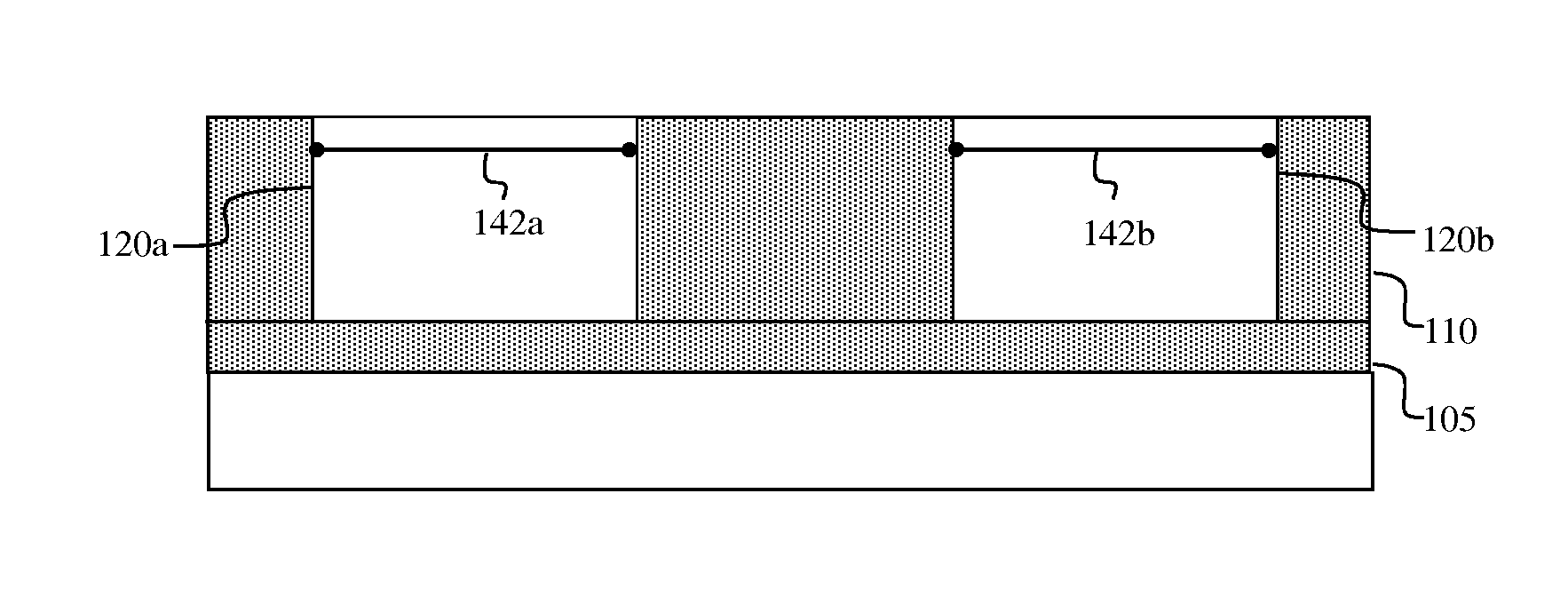
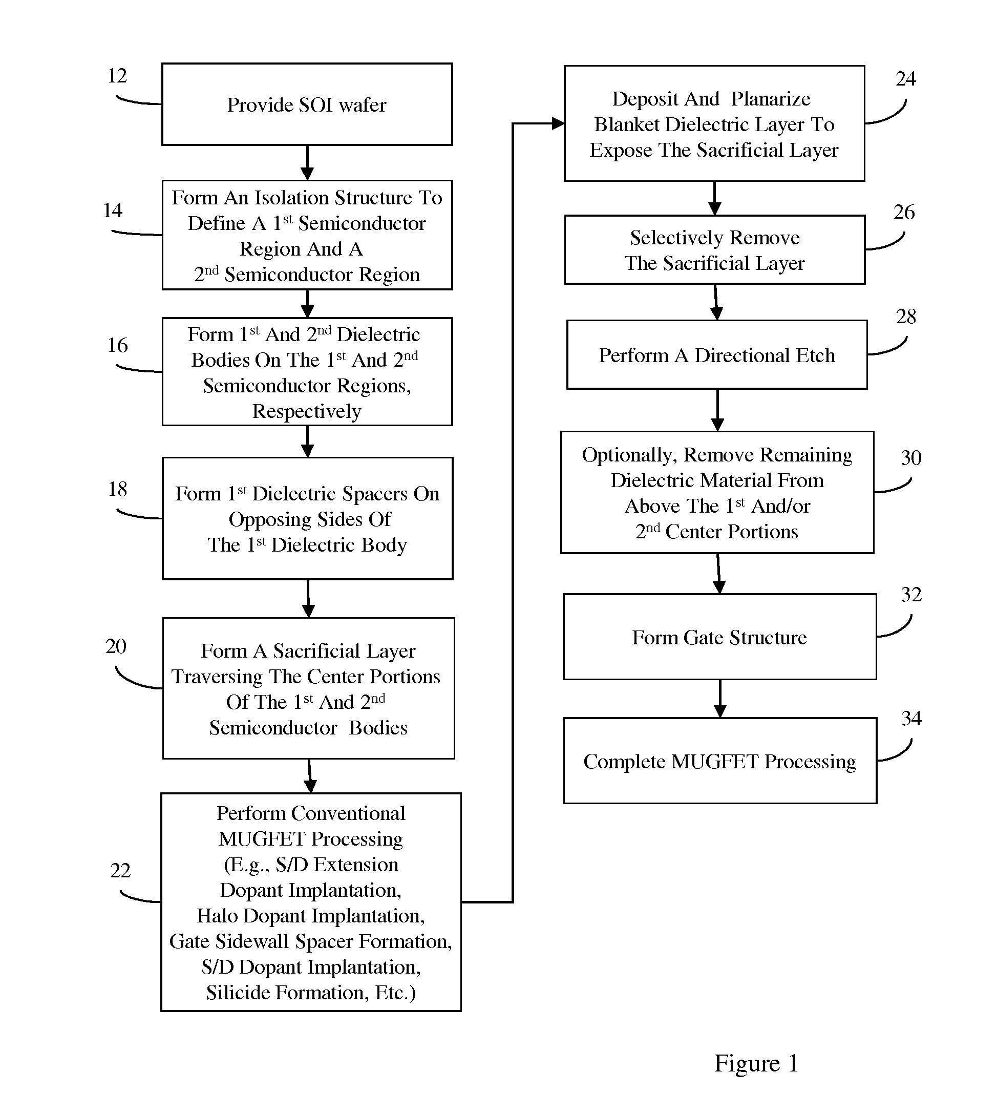
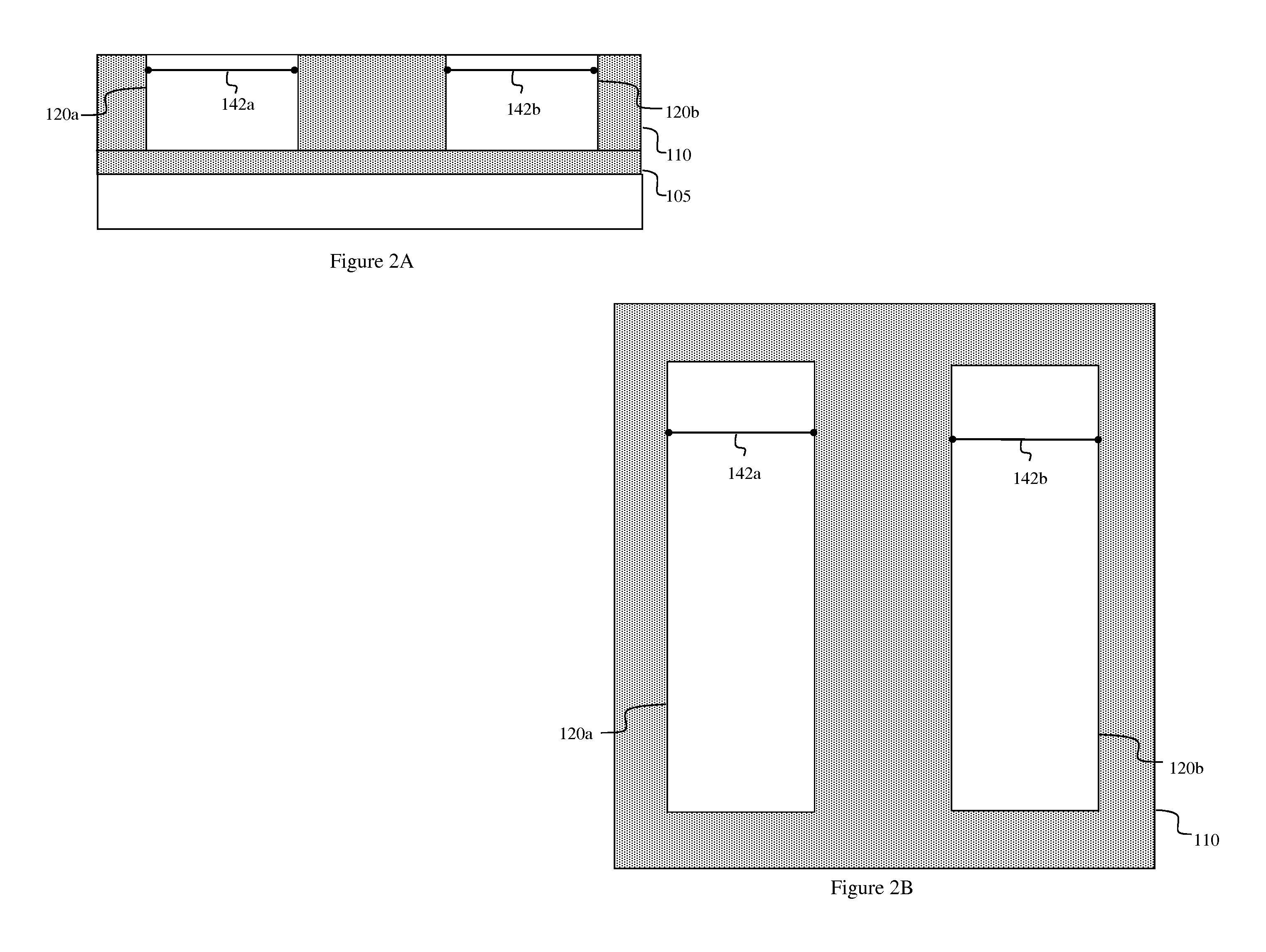
[0062]As discussed above, integrated circuit design decisions are often driven by device scalability and manufacturing efficiency. For example, because size scaling of planar field effect transistors (FETs) resulted in reduced drive current as a function of reduced channel width, non-planar multi-gate field effect transistors (MUGFETs) (e.g., dual-gate FETs and tri-gate FETs) were developed to provide scaled devices with increased drive current and reduced short channel effects. A dual-gate FET (also referred to as a fin-type FET or FINFET) is a non-planar FET comprising a relatively thin semiconductor fin with a channel region at the center of the fin positioned laterally between source / drain regions at the ends of the fin. A...


PUM


Abstract

Disclosed is a damascene method for forming a semiconductor structure and the resulting semiconductor structure having multiple fin-shaped channel regions with different widths. In the method, fin-shaped channel regions are etched using differently configured isolating caps as masks to define the different widths. For example, a wide width isolating cap can comprise a dielectric body positioned laterally between dielectric spacers and can be used as a mask to define a relatively wide width channel region; a medium width isolating cap can comprise a dielectric body alone and can be used as a mask to define a medium width channel region and/or a narrow width isolating cap can comprise a dielectric spacer alone and can be used as a mask to define a relatively narrow width channel region. These multiple fin-shaped channel regions with different widths can be incorporated into either multiple multi-gate field effect transistors (MUGFETs) or a single MUGFET.

Description

BACKGROUND[0001]1. Field of the Invention[0002]The present invention relates to embodiments of a damascene method of forming a semiconductor structure and to embodiments of a semiconductor structure with multiple fin-shaped channel regions having different widths.[0003]2. Description of the Related Art[0004]Integrated circuit design decisions are often driven by device scalability and manufacturing efficiency. For example, because size scaling of planar field effect transistors (FETs) resulted in reduced drive current as a function of reduced channel width, non-planar multi-gate field effect transistors (MUGFETs) (e.g., dual-gate FETs and tri-gate FETs) were developed to provide scaled devices with increased drive current and reduced short channel effects. A dual-gate FET (also referred to as a fin-type FET or FINFET) is a non-planar FET comprising a relatively thin semiconductor fin with a channel region at the center of the fin positioned laterally between source / drain regions at ...

Claims


Application Information

Patent Timeline
Patent Type & Authority Applications(United States)
IPC IPC(8): H01L29/02H01L21/70
CPCH01L29/785H01L29/66795
Inventor ANDERSON, BRENT A.NOWAK, EDWARD J.RANKIN, JED H.
Owner GLOBALFOUNDRIES INC
Why Eureka
Try Eureka