Clock gating for system-on-chip elements

a technology of hardware elements and clock gating, which is applied in the field of interconnect architecture, can solve the problems of complex routing form, inability to analyze and implement routing, and the inability to meet the requirements of dimension order routing, so as to reduce latency penalty, save power, and reduce latency penalty

Active Publication Date: 2017-02-14
TAHOE RES LTD
View PDF78 Cites 38 Cited by
  • Summary
  • Abstract
  • Description
  • Claims
  • Application Information

AI Technical Summary

Benefits of technology

[0024]An aspect of the present disclosure provides a hardware element in a Network on Chip (NoC) and a System on Chip (SoC), wherein the hardware element includes a clock gating circuit configures one or more neighboring hardware elements to activate before receiving new incoming data and to sleep after a defined number of cycles, wherein the defined number of cycles can be counted from a cycle having non-receipt of incoming data and having a clearance of all data within an input queue of a source hardware element. In an embodiment, the defined number of cycles can be set based on at least one of a predetermined number of cycles, say 3 or 4 cycles. In another embodiment, the defined number of cycles can be set based a self-learning process associated with one or more conditions of the system. In yet another embodiment, the number of cycles can be configured based on a hysteresis counter for reducing latency penalty due to clock gating and for saving power, wherein the hysteresis counter value can be configured to be set via self-learning based on network traffic and SoC and NoC conditions, and wherein the self-learning applies self-correction to the number of cycles. Any other process / attribute / factor can be incorporated for computing the number of cycles, post which the concerned hardware elements such as routers, bridges, can go to sleep.
[0025]Another aspect of the present disclosure provides a semiconductor device incorporating a Network on Chip (NoC) and a System on Chip (SoC), wherein the NoC and SoC includes a hardware element having a clock gating circuit configures one or more neighboring hardware elements to activate before receiving new incoming data and to sleep after a defined number of cycles, wherein the defined number of cycles can be counted from a cycle having non-receipt of incoming data and having a clearance of all data within an input queue of a source hardware element. In an embodiment, the defined number of cycles can be set based on at least one of a predetermined number of cycles, say 3 or 4 cycles. In another embodiment, the defined number of cycles can be set based a self-learning process associated with one or more conditions of the SoC and NoC. In yet another embodiment, the number of cycles can be configured based on a hysteresis counter for reducing latency penalty due to clock gating and for saving power, wherein the hysteresis counter value can be configured to be set via self-learning based on network traffic and SoC and NoC conditions, and wherein the self-learning applies self-correction to the number of cycles. Any other process / attribute / factor can be incorporated for computing the number of cycles, post which the concerned hardware elements such as routers, bridges, can go to sleep.

Problems solved by technology

The number of components on a chip is rapidly growing due to increasing levels of integration, system complexity, and shrinking transistor geometry.
In heterogeneous mesh topology in which one or more routers or one or more links are absent, dimension order routing may not be feasible between certain source and destination nodes, and alternative paths may have to be taken.
This form of routing may be complex to analyze and implement.
Based upon the traffic between various end points, and the routes and physical networks that are used for various messages, different physical channels of the NoC interconnect may experience different levels of load and congestion.
Unfortunately, channel widths cannot be arbitrarily large due to physical hardware design restrictions, such as timing or wiring congestion.
There may be a limit on the maximum channel width, thereby putting a limit on the maximum bandwidth of any single NoC channel.
Additionally, wider physical channels may not help in achieving higher bandwidth if messages are short.
Due to these limitations on the maximum NoC channel width, a channel may not have enough bandwidth in spite of balancing the routes.
With such a large variety of design choices, determining the right combination of routers, channels, and interconnections for a given system remains a challenge and time consuming manual process, often resulting in sub-optimal and inefficient designs.
This is necessary because NoC-style interconnects are distributed systems and their dynamic performance characteristics under load are difficult to predict statically and can be very sensitive to a wide variety of parameters.

Method used


Image

  • Clock gating for system-on-chip elements
  • Clock gating for system-on-chip elements
  • Clock gating for system-on-chip elements

Examples


Embodiment Construction

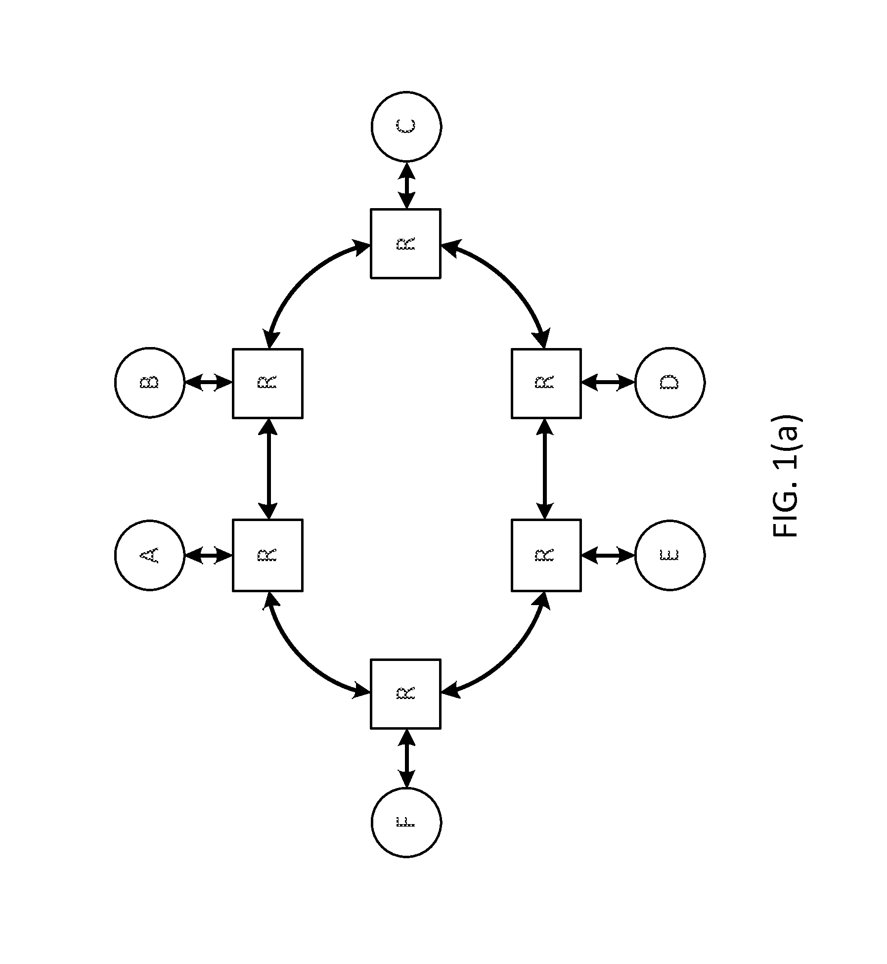
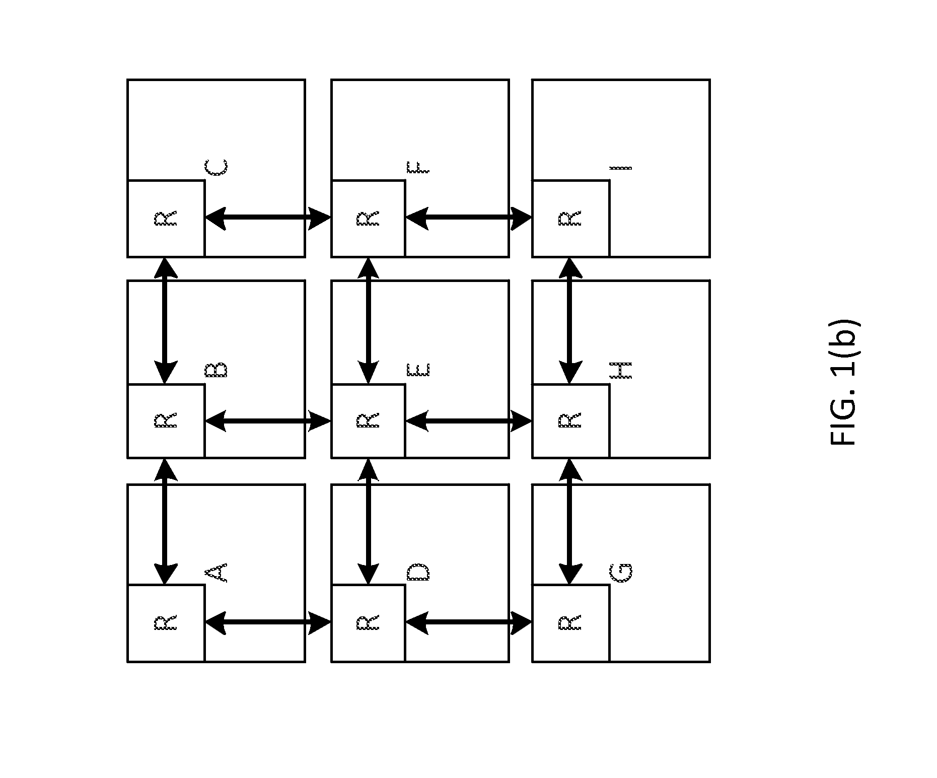
[0036]Although example implementations are described herein with respect to a NoC, the same implementations can be implemented in a SoC or in a system incorporating both a SoC and a NoC.

[0037]The following detailed description provides further details of the figures and example implementations of the present application. Reference numerals and descriptions of redundant elements between figures are omitted for clarity. Terms used throughout the description are provided as examples and are not intended to be limiting. For example, the use of the term “automatic” may involve fully automatic or semi-automatic implementations involving user or administrator control over certain aspects of the implementation, depending on the desired implementation of one of ordinary skill in the art practicing implementations of the present application.

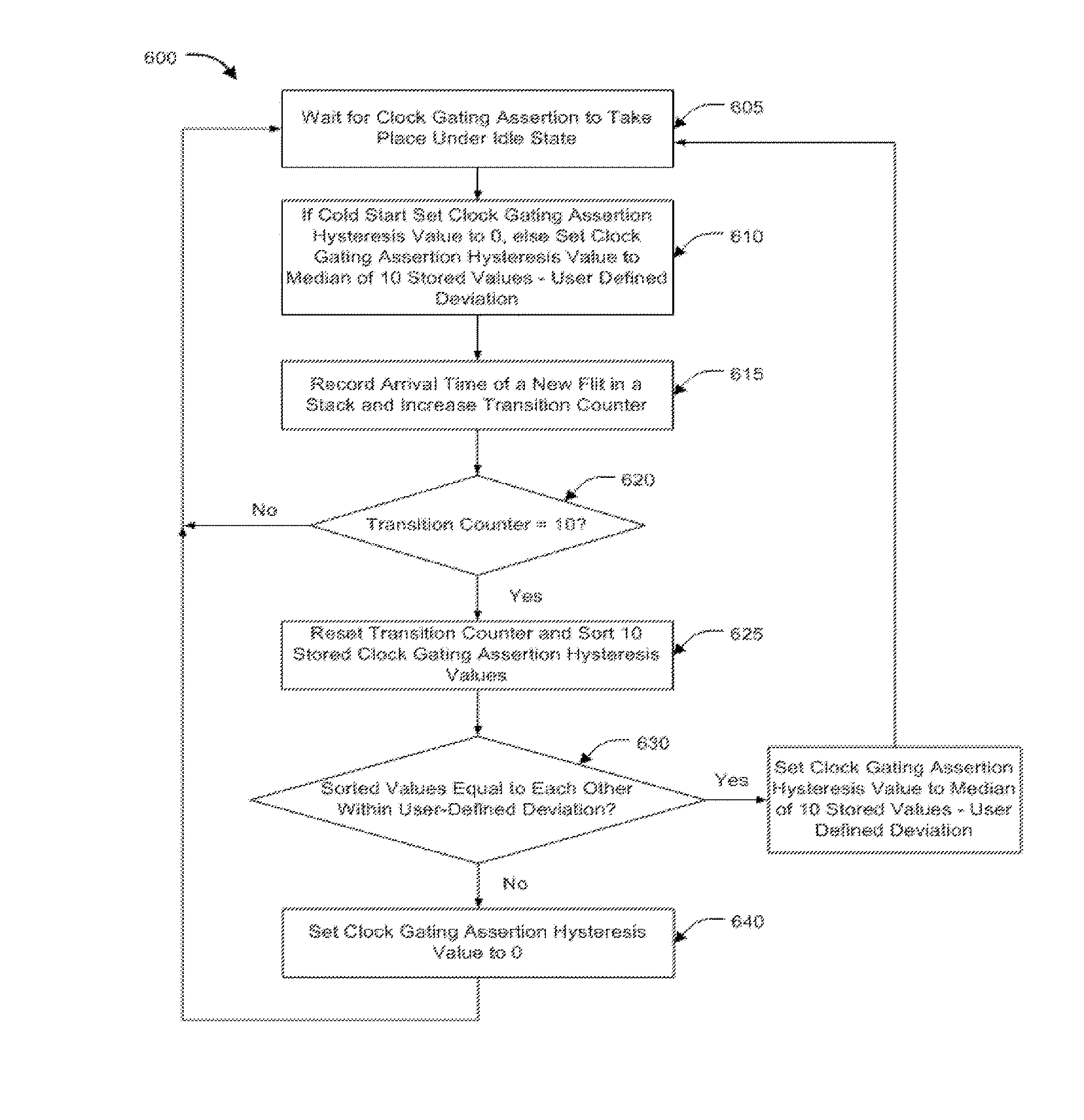
[0038]Example implementations involve clocked floating point operations (FLOPS) within the NoC. When there is no data on the activity side for a long time...


PUM


Abstract

An aspect of the present disclosure provides a hardware element in a Network on Chip (NoC), wherein the hardware element includes a clock gating circuit configures one or more neighboring hardware elements to activate before receiving new incoming data and to sleep after a defined number of cycles, wherein the defined number of cycles can be counted from a cycle having non-receipt of incoming data and/or having a clearance of all data within an input queue of a source hardware element.

Description

BACKGROUND[0001]Technical Field[0002]Methods and example implementations described herein are generally directed to interconnect architecture, and more specifically, to clock gating for hardware elements on a System on Chip (SoC) and Network on Chip (NoC), interconnecting them[0003]Related Art[0004]The number of components on a chip is rapidly growing due to increasing levels of integration, system complexity, and shrinking transistor geometry. Complex System-on-Chips (SoCs) may involve a variety of components e.g., processor cores, DSPs, hardware accelerators, memory and I / O, while Chip Multi-Processors (CMPs) may involve a large number of homogenous processor cores, memory and I / O subsystems. In both SoC and CMP systems, the on-chip interconnect plays a role in providing high-performance communication between the various components. Due to scalability limitations of traditional buses and crossbar based interconnects, Network-on-Chip (NoC) has emerged as a paradigm to interconnect ...

Claims


Application Information

Patent Timeline
Patent Type & Authority Patents(United States)
IPC IPC(8): G06F17/50H04L12/803H04L12/751H04L12/24H04L12/933G06N20/00H04L45/02
CPCH04L41/0816H04L41/0833H04L45/08H04L49/109H04L47/125H04L12/12H04L41/08Y02D30/50G06N20/00G06F1/32G06N5/045
Inventor KUMAR, SAILESHDAS, SANDIPKONGETIRA, POONACHA
Owner TAHOE RES LTD
Why Eureka
Try Eureka