Light emitting element

a technology of light-emitting elements and electrodes, which is applied in the direction of basic electric elements, electrical equipment, semiconductor devices, etc., can solve the problems of insufficient emission to achieve uniformity, and achieve the effect of reducing the uneven distribution of current density between electrodes

Active Publication Date: 2017-02-21
NICHIA CORP
View PDF42 Cites 16 Cited by
  • Summary
  • Abstract
  • Description
  • Claims
  • Application Information

AI Technical Summary

Benefits of technology

[0007]Accordingly, the present disclosure is devised to solve the problems as described above, and is aimed to provide a light emitting element reducing uneven distribution of the current density between the electrodes.
[0009]With the light emitting element according to the present disclosure, uneven distribution of the current density between the electrodes can be reduced.

Problems solved by technology

However, even with those structures, a deviation in the distribution of current density within a region disposing between the second electrode and the first electrode occurs, which may cause concern of insufficient for obtaining a uniform emission.

Method used


Image

  • Light emitting element
  • Light emitting element
  • Light emitting element

Examples


example 1

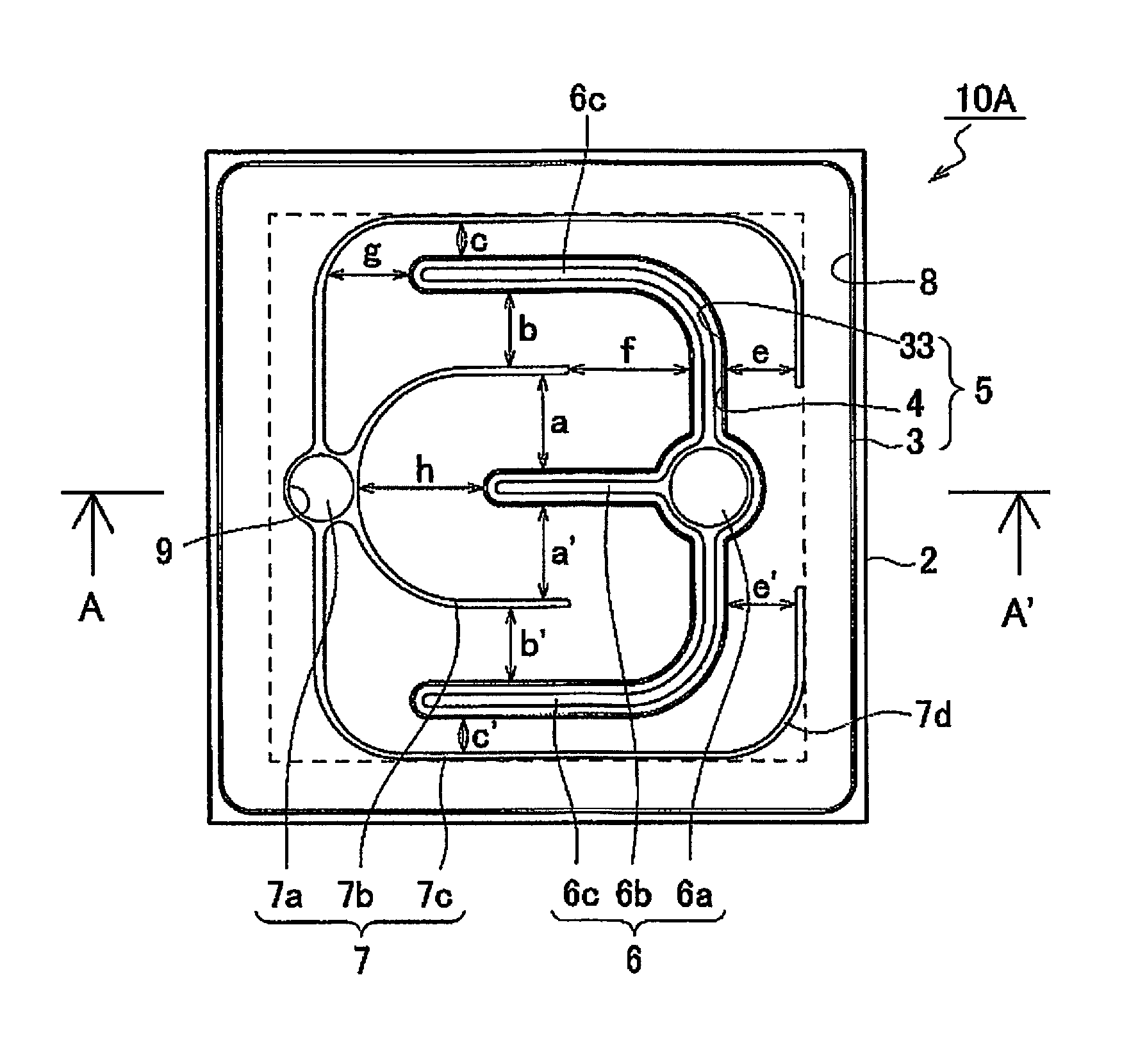
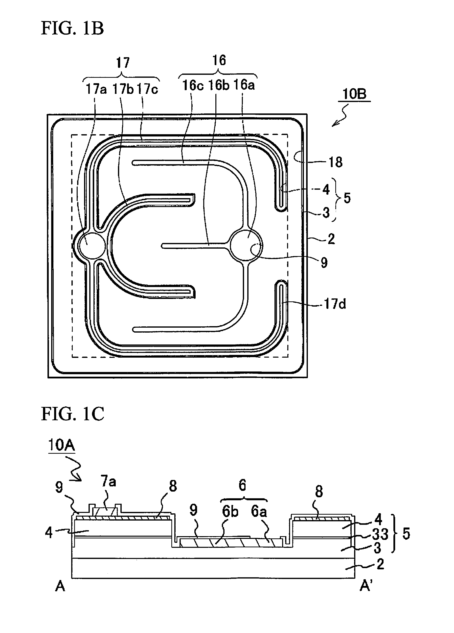
[0088]As shown in FIGS. 1A and 1C, the light emitting element 10A in Example 1 has a substrate 2, a semiconductor stack 5 having an n-type semiconductor layer 3 (a first conductivity type semiconductor layer), an active layer 33, and a p-type semiconductor layer 4 (a second conductivity type semiconductor layer) provided in that order over the substrate 2, an n-side electrode (a first electrode 6) formed on the n-type semiconductor layer 3, and a p-side electrode (a second electrode 7) that is disposed on the p-type semiconductor layer 4 and surrounding the n-side electrode.

[0089]The substrate 2 and the semiconductor stack 5 (in particular, the p-type semiconductor layer 4) has an approximately square shape in a plan view, the length of a side of the semiconductor stack 5 or the substrate 2 is 800 μm.

[0090]The first electrode 6 (the n-side electrode) is formed on the n-type semiconductor layer 3 at the part of the semiconductor stack 5 exposed by removing part of the p-type semicond...

modification example 1 of example 1

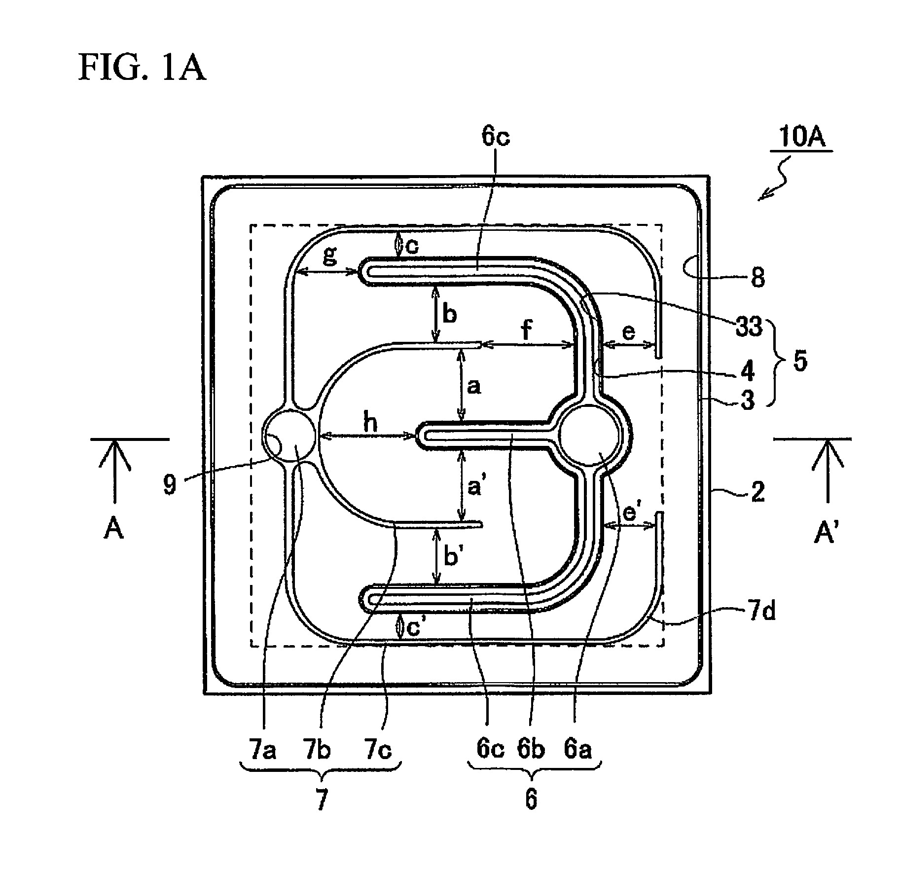
[0109]As shown in FIG. 1B, the light emitting element 10B of this Modification Example 1 of Example 1 has substantially the same configuration as the light emitting element 10A in Example 1, except that the first electrode 16 is the p-side electrode, and the second electrode 17 is the n-side electrode.

[0110]That is, the light emitting element 10B has a first electrode 16 as the p-side electrode, which has a first connecting portion 16a, a first extending portion 16b, and two second extending portions 16c. The light emitting element 10B has a second electrode 17 as the n-side electrode, which has a second connecting portion 17a, two third extending portions 17b, and two fourth extending portions 17c. The distal ends 17d of these fourth extending portions 17c are bent toward the first connecting portion 16a.

[0111]The width of the first extending portion 16b is 12 μm.

[0112]The width of the second extending portion 16c is 12 μm.

[0113]The width of the third extending portion 17b is 8 μm...

modification example 2 of example 1

[0115]As shown in FIG. 1D, the light emitting element 10C of this Modification Example 2 of Example 1 is similar to the light emitting element 10A in that the second connecting portion 7a, the third extending portions 7b, and the fourth extending portions 7c are disposed at the second electrode 7, and has substantially the same configuration as the light emitting element 1 OA in Example 1 except that the distal ends of the fourth extending portions 7c are not bent, and extend linearly toward the end of the light emitting element 10C, past the outermost end of the first connecting portion 6a.

[0116]The distance between the distal ends of the fourth extending portions 7c near the end of the light emitting element and the end of the semiconductor stack 5 in the direction in which the fourth extending portions 7c extend parallel to the first extending portion 6b is 62 μm.


PUM


Abstract

A light emitting element having; a first and a second conductivity type semiconductor layers, a first and a second electrodes formed on the first and second conductivity type semiconductor layer, the first and the second electrodes being disposed on the same face side of the first conductivity type semiconductor layer and the second conductivity type semiconductor layer, in plan view, the first electrode having a first connecting portion, a first extending portion, and two second extending portions, the second electrode having a second connecting portion and two third extending portions, the first extending portion of the first electrode extending linearly from the first connecting portion toward the second connecting portion, and the two second extending portions extending parallel to the first extending portion on two sides of the first extending portion, the two third extending portions of the second electrode extending parallel to the first extending portion between the first extending portion and the two second extending portions.

Description

CROSS-REFERENCE TO RELATED APPLICATIONS[0001]This application claims priority to Japanese Patent Application No. 2013-254243 filed on Dec. 9, 2013 and Japanese Patent Application No. 2014-236462 filed on Nov. 21, 2014. The entire disclosure of Japanese Patent Application No. 2013-254243 and No. 2014-236462 are hereby incorporated herein by reference.BACKGROUND[0002]Technical Field[0003]The present disclosure relates to a light emitting element, and particularly to an electrode structure of the light emitting element.[0004]Related Art[0005]There have been made various developments to obtain a uniform emission from a light emitting element. For example, for a light emitting element having a quadrilateral outer shape, electrode structures in which either a second electrode or a first electrode is disposed at a center portion of an upper surface of a light emitting element, and the other electrode is disposed embracing it (for example, JP 2011-61077 A, JP 2012-89695 A and JP 2011-139037...

Claims


Application Information

Patent Timeline
Patent Type & Authority Patents(United States)
IPC IPC(8): H01L33/00H01L33/38
CPCH01L33/387H01L33/38H01L33/06
Inventor SATO, KOSUKEEMURA, KEIJI
Owner NICHIA CORP
Why Eureka
Try Eureka