
Multilayer body
- Summary
- Abstract
- Description
- Claims
- Application Information
AI Technical Summary
Benefits of technology
Problems solved by technology
Method used
Image

Examples
Embodiment Construction
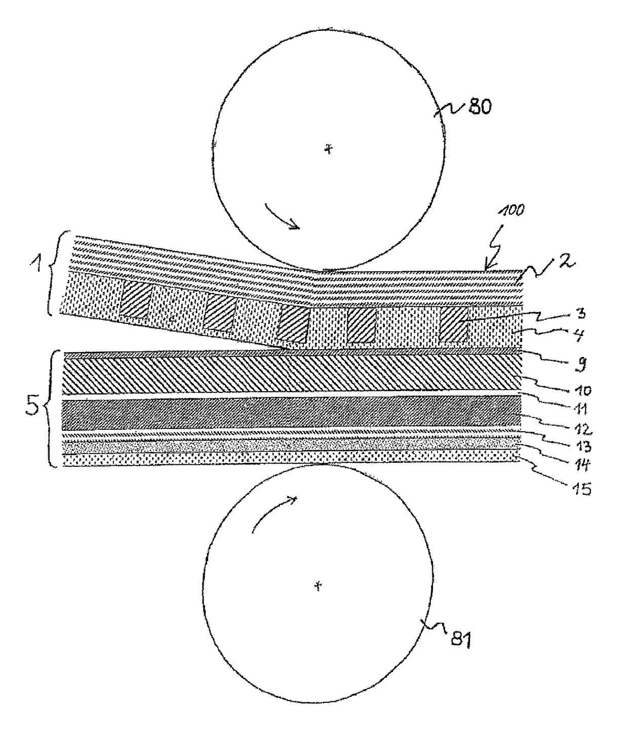
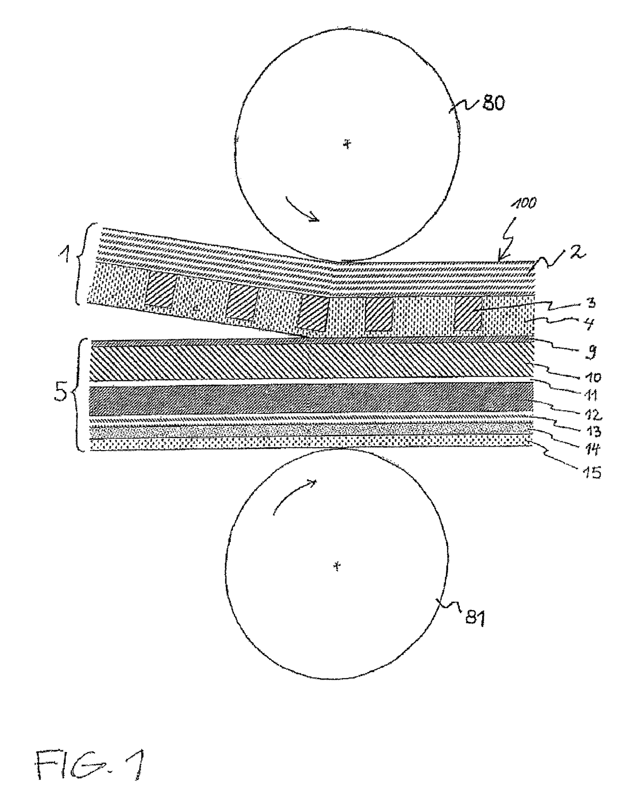
[0079]FIG. 1 shows a process for producing a multilayer body 100. Provided for this is a relief film 1, which has a first carrier film 2 and a structural layer 3 arranged on one side of the first carrier film 2. In the present exemplary embodiment, the structural layer 3 is formed as a lacquer layer printed onto the first carrier film 2 by means of screen printing. Therefore, the first carrier film 2 has a region that is covered by the structural layer 3 and a largely uncovered region; the structural layer 3 is therefore formed in specific regions, i.e. partially. Furthermore, the relief film 1 has an adhesive layer 4, which has been applied to the partially arranged structural layer 3 and which covers the structural layer 3 on its side facing away from the carrier film 2. The first carrier film 2 of the relief film 1 has a thickness in the range from 12 to 50 μm, preferably in the range from 16 to 23 μm. In this figure, as in the other figures, the devices represented are not shown...
PUM
| Property | Measurement | Unit |
|---|---|---|
| Thickness | aaaaa | aaaaa |
| Thickness | aaaaa | aaaaa |
| Thickness | aaaaa | aaaaa |
Abstract
Description
Claims
Application Information