Etching method and bevel etching apparatus

a bevel etching and etching technology, which is applied in the direction of laser beam welding apparatus, semiconductor/solid-state device testing/measurement, manufacturing tools, etc., can solve the problems of affecting the output intensity of laser beam, and affecting the quality of laser beam

Active Publication Date: 2017-04-18
TOKYO ELECTRON LTD
View PDF4 Cites 3 Cited by
  • Summary
  • Abstract
  • Description
  • Claims
  • Application Information

AI Technical Summary

Benefits of technology

[0008]Accordingly, in response to the above discussed problems, embodiments of the present invention aim to provide an etching method and a bevel etching apparatus that monitor a laser beam before emitted to a bevel portion of a substrate and detect variation of an output of the laser beam.

Problems solved by technology

However, even when the current supplied to the laser generator is constant, the output intensity of the laser beam varies due to a malfunction or a temporal change of the laser generator.
When an output value of the laser beam is out of order and the failure cannot be detected, the bevel portion of the wafer is liable to be irradiated with the laser beam having power higher than a prescribed value, and is liable to be scraped and chipped.

Method used


Image

  • Etching method and bevel etching apparatus
  • Etching method and bevel etching apparatus
  • Etching method and bevel etching apparatus

Examples


Embodiment Construction

[0022]A description is given below of embodiments of the present invention, with reference to accompanying drawings. Note that elements having substantially the same configuration may be given the same reference numerals and overlapping descriptions thereof may be omitted.

[0023][Introduction]

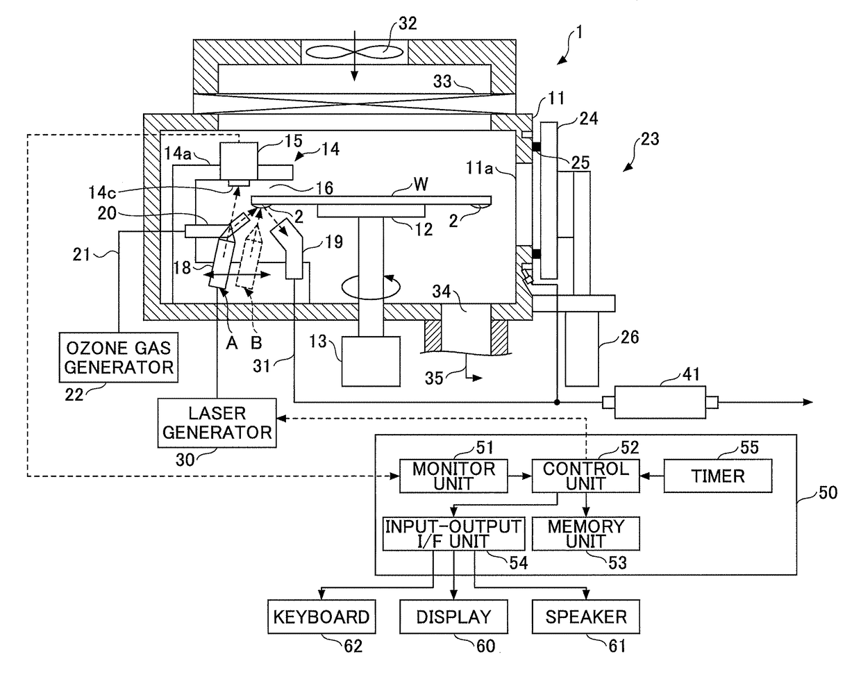
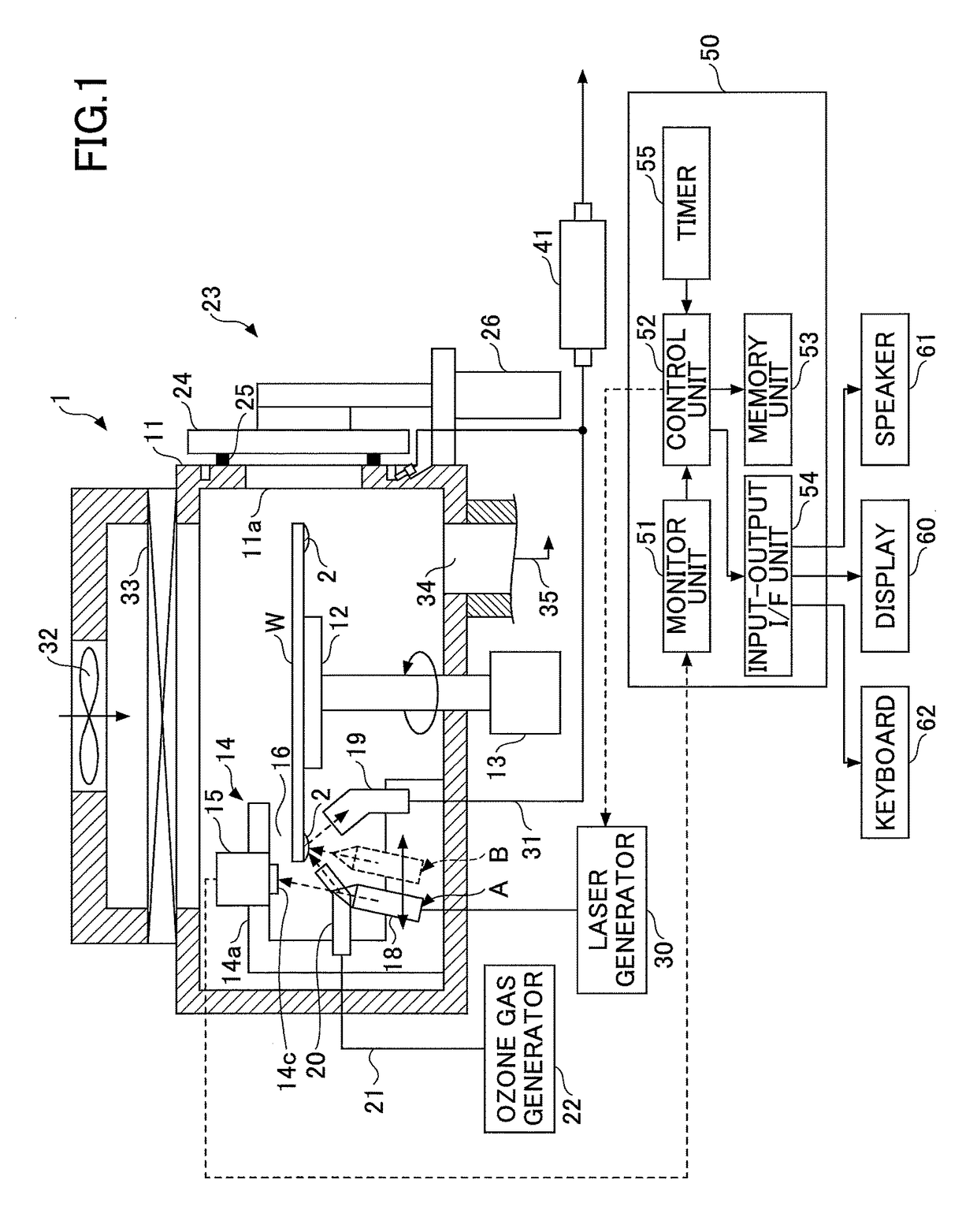
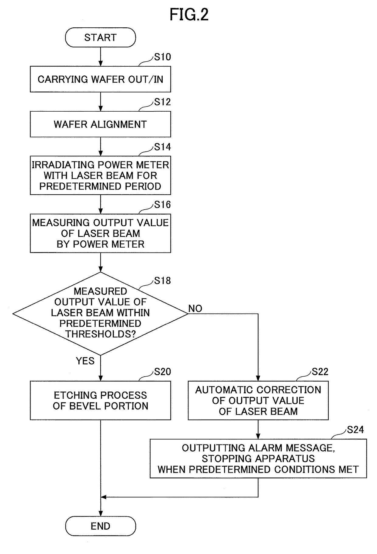
[0024]In manufacturing semiconductor integrated circuits, when a plasma etching is performed on a wafer, radicals and ions generated in plasma go around to a bevel surface of a back surface of the wafer, and a polymer attaches to the bevel surface and the back surface of the wafer. The attachments are called a bevel / backside polymer (which is hereinafter called a “BSP”). The BSP contaminates a surface of a semiconductor integrated circuit device or affects a yield rate of a product. Therefore, the BSP is removed by a heat treatment using a laser beam and ozone gas. A description is given below of an embodiment of a bevel etching apparatus for removing the BSP.

[0025][Overall Configuration of Beve...


PUM

PropertyMeasurementUnit
timeaaaaaaaaaa
timeaaaaaaaaaa
power meteraaaaaaaaaa

Abstract

An etching method using a bevel etching apparatus is provided. The bevel etching apparatus is configured to etch a substrate by emitting a laser beam and includes a laser generator and a power meter configured to measure the laser beam output from the laser generator. In the method, the power meter is irradiated with the laser beam for a predetermined period of time before etching the substrate by irradiating the substrate with the laser beam. An output value of the laser beam is measured by the power meter. It is determined whether the measured output value of the laser beam is in a range of predetermined thresholds with respect to an output setting value of the laser beam output from the laser generator.

Description

CROSS-REFERENCE TO RELATED APPLICATIONS[0001]This patent application is based upon and claims the benefit of priority of Japanese Patent Application No. 2014-118946, filed on Jun. 9, 2014, the entire contents of which are incorporated herein by reference.BACKGROUND OF THE INVENTION[0002]1. Field of the Invention[0003]The present invention relates to an etching method and a bevel etching apparatus.[0004]2. Description of the Related Art[0005]A bevel / backside polymer attached to a bevel portion (chamfered portion of a wafer edge) of a semiconductor wafer (which may be hereinafter just called a “wafer”) contaminates a surface of a device or affects a yield rate of a product.[0006]In response to this, Japanese Laid-Open Patent Application Publication No. 2010-141237 proposes an apparatus that irradiates a bevel portion of a wafer with a laser beam, thereby removing a bevel / backside polymer by etching. The output intensity of the laser beam emitted to the bevel portion is managed by moni...

Claims


Application Information

Patent Timeline
Patent Type & Authority Patents(United States)
IPC IPC(8): H01L21/00B23K26/06H01L21/67B23K26/30B23K26/362B23K26/36H01L21/66B23K26/40H01L21/02
CPCB23K26/0626B23K26/362H01L21/6708H01L21/67115H01L21/67253H01L22/00H01L21/02087H01L21/02021B23K26/361
Inventor KONDO, MASAKI
Owner TOKYO ELECTRON LTD
Why Eureka
Try Eureka