Supercharge Your Innovation With Domain-Expert AI Agents!

Semiconductor device performing error correction operation

a technology of error correction and semiconductor devices, applied in the field of semiconductor devices, can solve the problems of increased and increased probability of failure, so as to reduce the probability of error occurren

Active Publication Date: 2017-04-18
SK HYNIX INC
View PDF5 Cites 0 Cited by
  • Summary
  • Abstract
  • Description
  • Claims
  • Application Information

AI Technical Summary

Benefits of technology

The semiconductor device described in this patent can correct errors that may occur during operation. When multiple devices are connected to form a memory channel, both the individual device and the memory controller can correct errors in data output from the channel, which further reduces the likelihood of errors.

Problems solved by technology

As such, the error correction block included in the memory controller does not perform the error correction operation in units of individual semiconductor memory devices.
Recently, as the cell size of a semiconductor memory device is reduced, the probability of error occurrence is increased.
Therefore, when an error correction operation is performed only in units of memory controllers, there is a problem that the probability of fail may increase due to errors that occur in a plurality of semiconductor memory devices connected to a memory channel.

Method used


Image

  • Semiconductor device performing error correction operation
  • Semiconductor device performing error correction operation
  • Semiconductor device performing error correction operation

Examples


Embodiment Construction

[0022]Hereinafter, a semiconductor device according to various embodiments will be described in detail with reference to the accompanying drawings through various examples of embodiments.

[0023]For example, a semiconductor device including memory cells and capable of performing an error correction operation therein may be described herein.

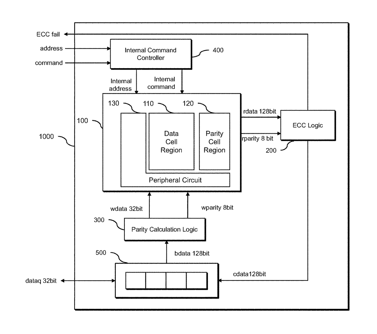
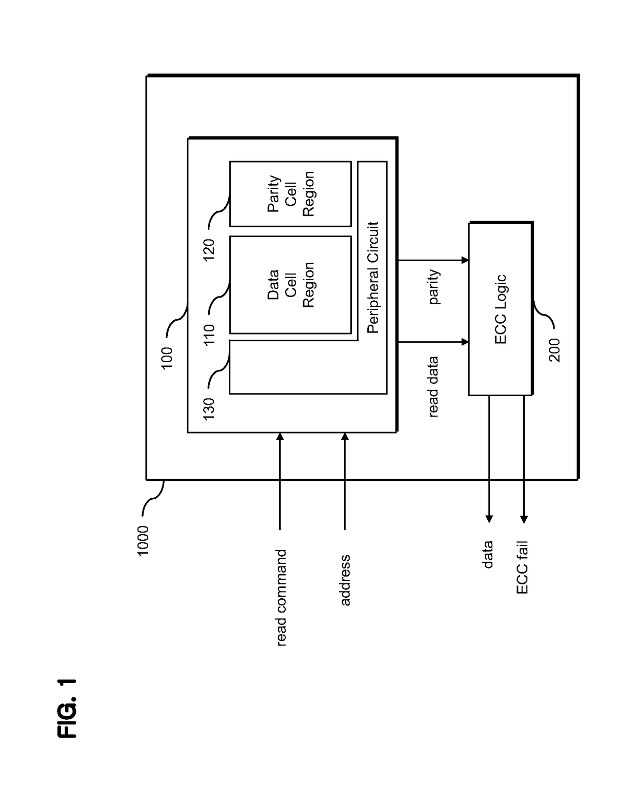
[0024]FIG. 1 is a block diagram representation illustrating a read operation of a semiconductor device 1000 according to an embodiment.

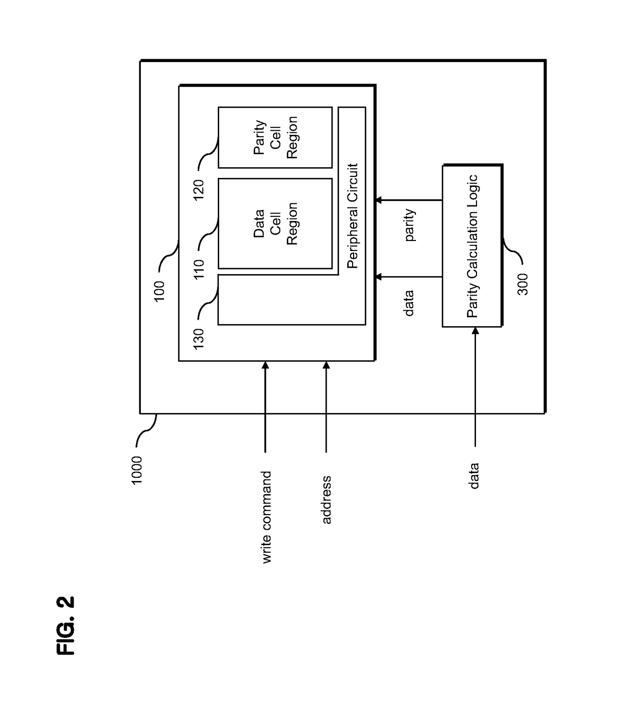
[0025]The semiconductor device 1000 according to an embodiment may include a memory core 100 and an ECC (Error Correcting Code) logic 200.

[0026]The memory core 100 may include a data cell region 110 that stores general data and a parity cell region 120 that stores a parity.

[0027]Since the data cell region 110 and the parity cell region 120 may be logically divided, the data cell region 110 and the parity cell region 120 may be physically positioned in a separate cell array or one cell array. For example, in a cell ar...


PUM


Abstract

A semiconductor device may include a memory core including a data cell region and a parity cell region, a parity calculation logic configured for generating a parity from data received by the parity calculation logic, and an error correcting logic configured for outputting error-corrected data by using data that is output from the data cell region and a parity that is output from the parity cell region.

Description

[0001]The present application claims priority under 35 U.S.C. §119(a) to Korean application number 10-2014-0011037, filed on Jan. 29, 2014, in the Korean Intellectual Property Office, which is incorporated herein by reference in its entirety as set forth in full.BACKGROUND[0002]1. Technical Field[0003]Various embodiments generally relate to a semiconductor device including memory cells. Particularly, the various embodiments relate to a semiconductor device capable of performing an error correction operation therein.[0004]2. Related Art[0005]In a conventional semiconductor memory devices error correction operations may be performed. For example, devices, such as a memory controller performing no error correction therein and controlling the semiconductor memory device, or a CPU, have performed an error correction operation.[0006]An error correction block included in the memory controller performs an error correction operation in units of a plurality of semiconductor memory devices con...

Claims


Application Information

Patent Timeline
Patent Type & Authority Patents(United States)
IPC IPC(8): H03M13/00G11C29/52G06F11/10G11C29/04
CPCG11C29/52G06F11/1008G11C2029/0411
Inventor CHOI, WON-HALEE, SEUNG-MIN
Owner SK HYNIX INC
Features
  • R&D
  • Intellectual Property
  • Life Sciences
  • Materials
  • Tech Scout
  • Unparalleled Data Quality
  • Higher Quality Content
  • 60% Fewer Hallucinations
Learn More