RF attenuator device and system

a technology of attenuator and resistive patch, which is applied in the direction of waveguide-type devices, electrical equipment, antenna earthing switches, etc., can solve the problems of limiting the rf bandwidth, and the ideal condition cannot be perfectly satisfied, so as to maximize the resistive patch arrangement, eliminate or significantly reduce the effect of attenuator circuit layout and simple attenuator circuit layou

Active Publication Date: 2017-04-25
TTM TECH INC
View PDF7 Cites 0 Cited by
  • Summary
  • Abstract
  • Description
  • Claims
  • Application Information

AI Technical Summary

Benefits of technology

[0016]The present invention addresses the needs described above by providing a different and simplified approach to manufacturing RF attenuator devices. The present invention features a simple attenuator circuit layout that substantially eliminates, or significantly reduces, the need to balance heat distribution between multiple resistors. Specifically, one embodiment of the attenuator circuit features a single resistor that substantially maximizes the resistive patch arrangement; i.e., it covers the maximum possible substrate surface area without degrading the input return loss. Thus, the present invention maximizes the device's power handling capabilities without sacrificing bandwidth. While solving the heat distribution issue, the present invention is configured to absorb the effects of parasitic capacitance and thus achieves a wideband return loss. Because the device layout features a single (bifurcated) resistor, it reduces the amount of laser trimming required to speed up the production process.

Problems solved by technology

Otherwise, the system components can overheat and become damaged.
On the other hand, when an attenuator device features relative large resistive film regions, the resistive sheets are characterized by large parasitic capacitances that limit the RF bandwidth.
Of course, since the attenuator 1 includes tuning circuitry such as transmission line TL, connecting lines and other layout constrains, the ideal condition cannot be perfectly satisfied.
Such laser trimming process adds time and, therefore, cost to the production process.

Method used


Image

  • RF attenuator device and system
  • RF attenuator device and system
  • RF attenuator device and system

Examples


Embodiment Construction

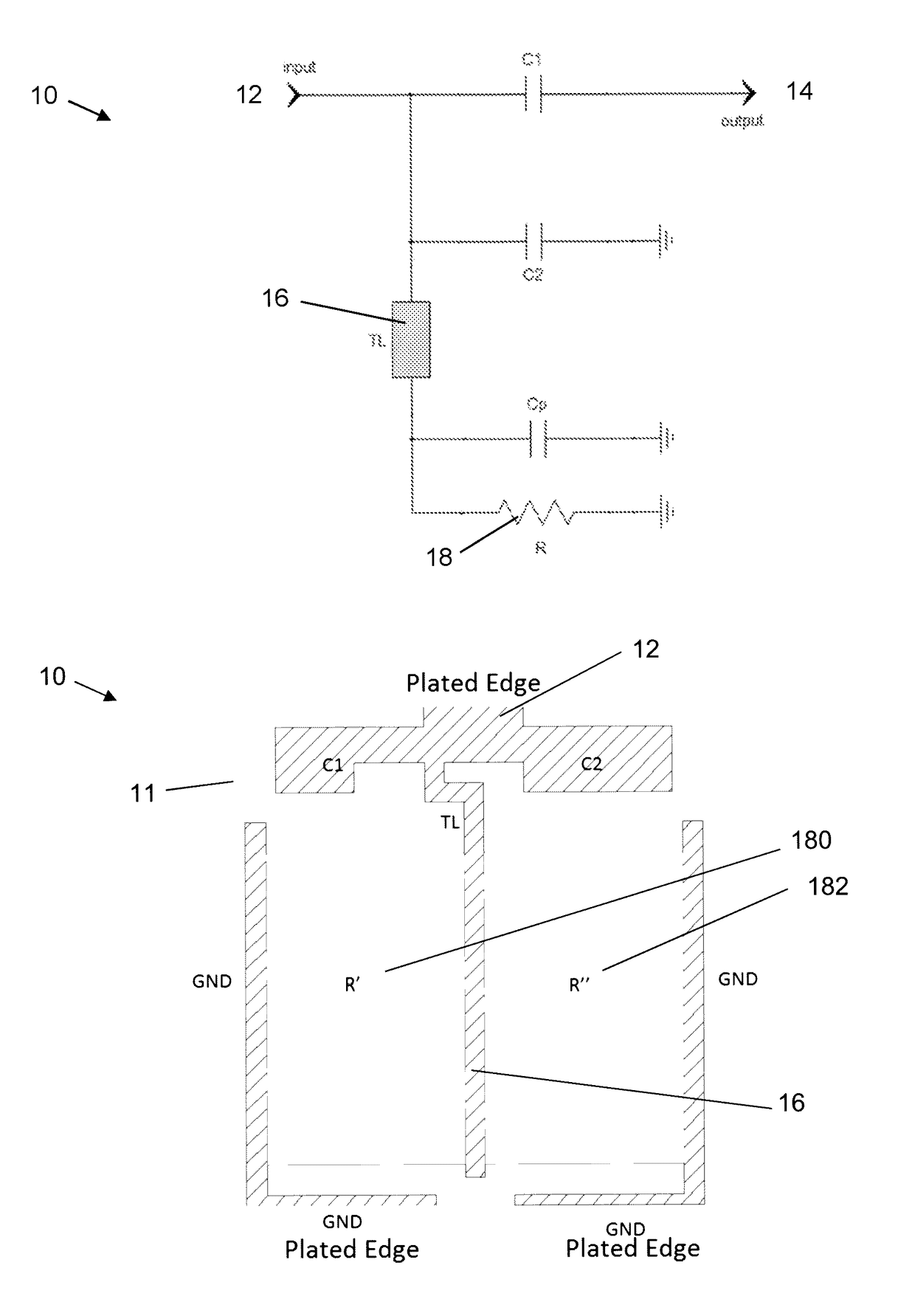
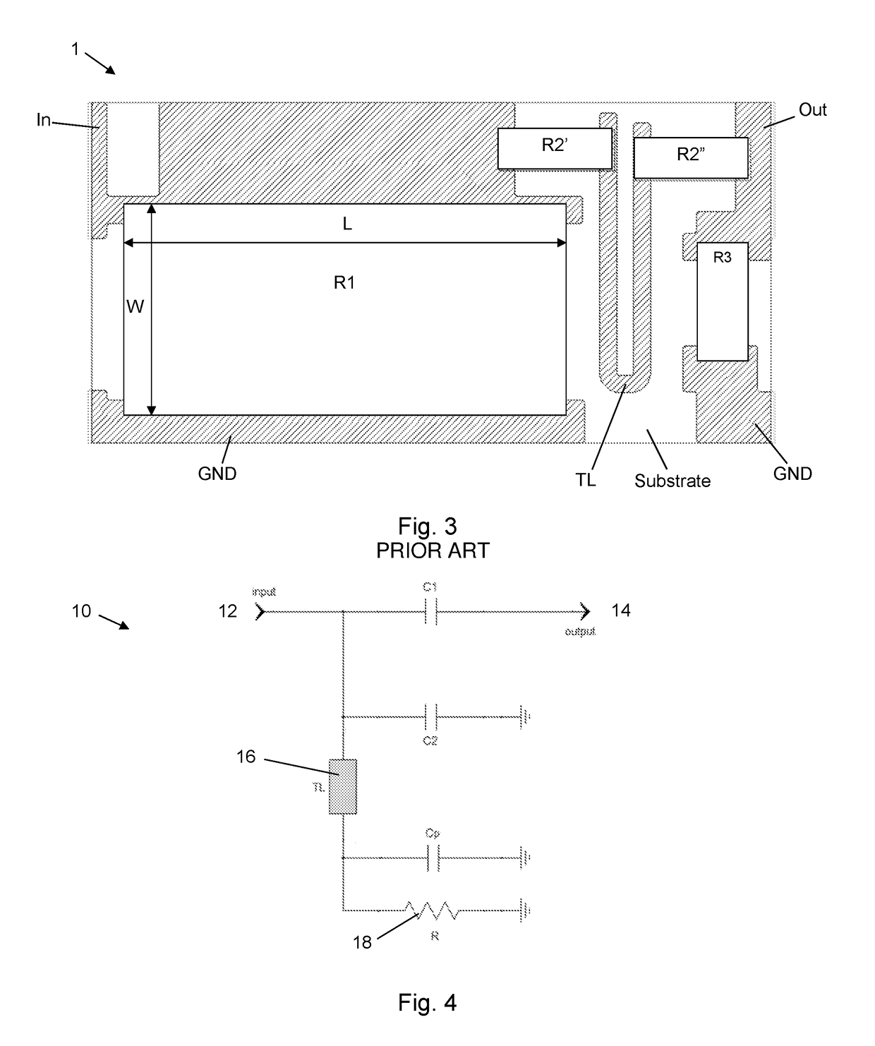
[0065]Reference will now be made in detail to the present exemplary embodiments of the invention, examples of which are illustrated in the accompanying drawings. Wherever possible, the same reference numbers will be used throughout the drawings to refer to the same or like parts. An exemplary embodiment of the attenuator of the present invention is shown in FIG. 4, and is designated generally throughout by reference numeral 10.

[0066]As embodied herein, and depicted in FIG. 4, a schematic view of an RF attenuator in accordance with an embodiment of the present invention is disclosed. In the schematic view of FIG. 4, a relatively small capacitor C1 is disposed between the input port 12 and the output port 14. Capacitor C1 is configured to couple a portion of the AC signal energy from the input port to output port. (Of course, capacitor C1 blocks DC signals). The input port 12 is also coupled to tuning capacitor C2 and inductive transmission line 16. The transmission line 16 is further...


PUM


Abstract

A device includes a thermally conductive and electrically insulative substrate having a first major surface and a second major surface. A coupling structure is configured to reduce the RF input signal by substantially a predetermined amount of attenuation power. A tuning circuit is characterized by a tuning reactance substantially matched to a predetermined system impedance. A resistor is disposed on a majority of the first major surface and is characterized by a parasitic capacitance that is substantially negated by the tuning reactance. The resistor includes a first resistive portion and a second resistive portion; each of the first resistive portion and the second resistive portion being configured to direct approximately one-half of the attenuation power to the ground portion.

Description

BACKGROUND OF THE INVENTION[0001]1. Field of the Invention[0002]The present invention relates generally to electrical devices and systems, and particularly to RF attenuators, devices and systems.[0003]2. Technical Background[0004]An RF attenuator is a device that is configured to reduce the level of an RF signal. Attenuation is typically measured as a ratio of the output power level over the input power level, and is thus given in decibels (dB). Because the power of the output signal is lower than the power of the input signal, the attenuation level is negative (e.g., −20 dB). As those of ordinary skill in the art will appreciate, attenuation is often required to protect a component or a circuit stage, e.g., monitoring or sampling circuitry, when an RF signal exceeds the power handling capabilities of the protected circuit. Thus, in many cases, the accuracy of the attenuator is important, because of the tolerances of the various stages of the overall RF design.[0005]RF attenuators r...

Claims


Application Information

Patent Timeline
Patent Type & Authority Patents(United States)
IPC IPC(8): H01Q1/50H03H7/25
CPCH03H7/25H01Q1/50H03H7/24H01P1/227
Inventor MEI, CHONGJENSEN, BO
Owner TTM TECH INC
Why Eureka
Try Eureka