Light-emitting element and light-emitting device

a technology of light-emitting elements and light-emitting devices, which is applied in the direction of solid-state devices, semiconductor devices, oled parameters, etc., can solve the problems of reducing the extraction efficiency of light from the light-emitting element, and achieves the reduction of power consumption, the increase of the extraction efficiency of light from the light-emitting element, and the effect of high visible light transmittan

Active Publication Date: 2017-05-09
SEMICON ENERGY LAB CO LTD
View PDF128 Cites 3 Cited by
  • Summary
  • Abstract
  • Description
  • Claims
  • Application Information

AI Technical Summary

Benefits of technology

[0009]In view of the foregoing technical background, an object of one embodiment of the present invention is to provide a light-emitting element capable of reducing power consumption by increasing its light extraction efficiency and a light-emitting device using the light-emitting element.
[0010]The present inventors have considered that the hole-injection property of a composite material containing an organic compound and a substance having an electron-accepting property with respect to the organic compound (hereinafter, referred to as electron acceptor) is not attributed to the charge-transfer complex formed through an oxidation-reduction reaction. In accordance with one embodiment of the present invention, even when a charge-transfer complex is not formed between the organic compound and the electron acceptor through the oxidation-reduction reaction, the excellent hole injection property can be ensured in such a way that holes generated through extraction of electrons from the organic compound by the electron acceptor on voltage application are injected from a layer containing the composite material into an adjacent layer.
[0014]Unlike in Patent Document 1, a composite material in which charge-transfer interaction does not occur easily between the organic compound and the electron acceptor is used in one embodiment of the present invention. Accordingly, the 300 nm to 600 nm wavelength light absorbed by a layer containing the above composite material due to charge-transfer interaction can be reduced, so that the transmittance of this layer for visible light having a wavelength of 360 nm to 830 nm can be increased.
[0019]In accordance with one embodiment of the present invention, a composite material having high visible light transmittance is used for a light-emitting element, so that the extraction efficiency of light from the light-emitting element can be increased. Thus, a light-emitting element capable of reducing power consumption and exhibiting high luminance and a light-emitting device using the light-emitting element can be provided.

Problems solved by technology

That means that the above charge generation layer absorbs light having a wavelength in the visible light region, which indicates that the charge-transfer complex included in the charge generation layer is one cause for a reduction in the extraction efficiency of light from the light-emissive element.

Method used


Image

  • Light-emitting element and light-emitting device
  • Light-emitting element and light-emitting device
  • Light-emitting element and light-emitting device

Examples


embodiment 1

[0048]A light-emitting element in accordance with one embodiment of the present invention includes at least one EL layer and a pair of electrodes between which the EL layer is provided. The EL layer contains a composite material which includes an organic compound having a high hole-transport property and an electron acceptor and in which charge-transfer interaction does not occur easily.

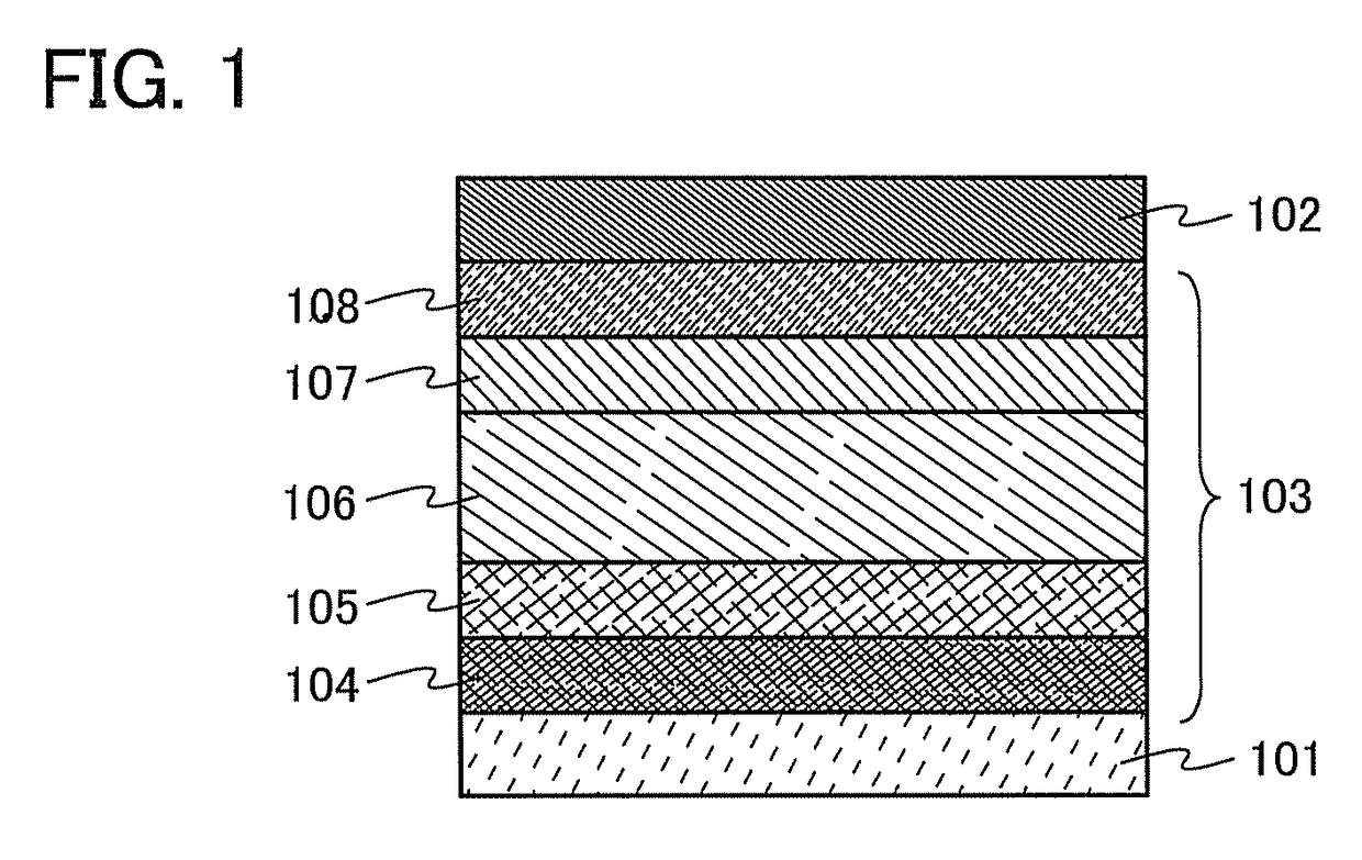
[0049]FIG. 1 illustrates a structure example of the light-emitting element in accordance with one embodiment of the present invention. The light-emitting element illustrated in FIG. 1 includes an anode 101 and a cathode 102, which correspond to the pair of electrodes, and an EL layer 103 provided between the anode 101 and the cathode 102.

[0050]In the example in FIG. 1, the EL layer 103 includes a hole-injection layer 104, a hole-transport layer 105, a light-emitting layer 106, an electron-transport layer 107, an electron-injection layer 108, and the like. Specifically, the hole-injection layer 104, t...

embodiment 2

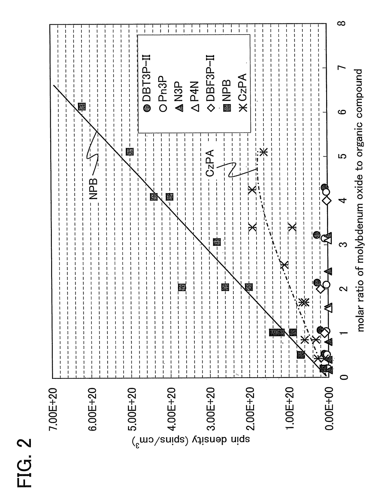
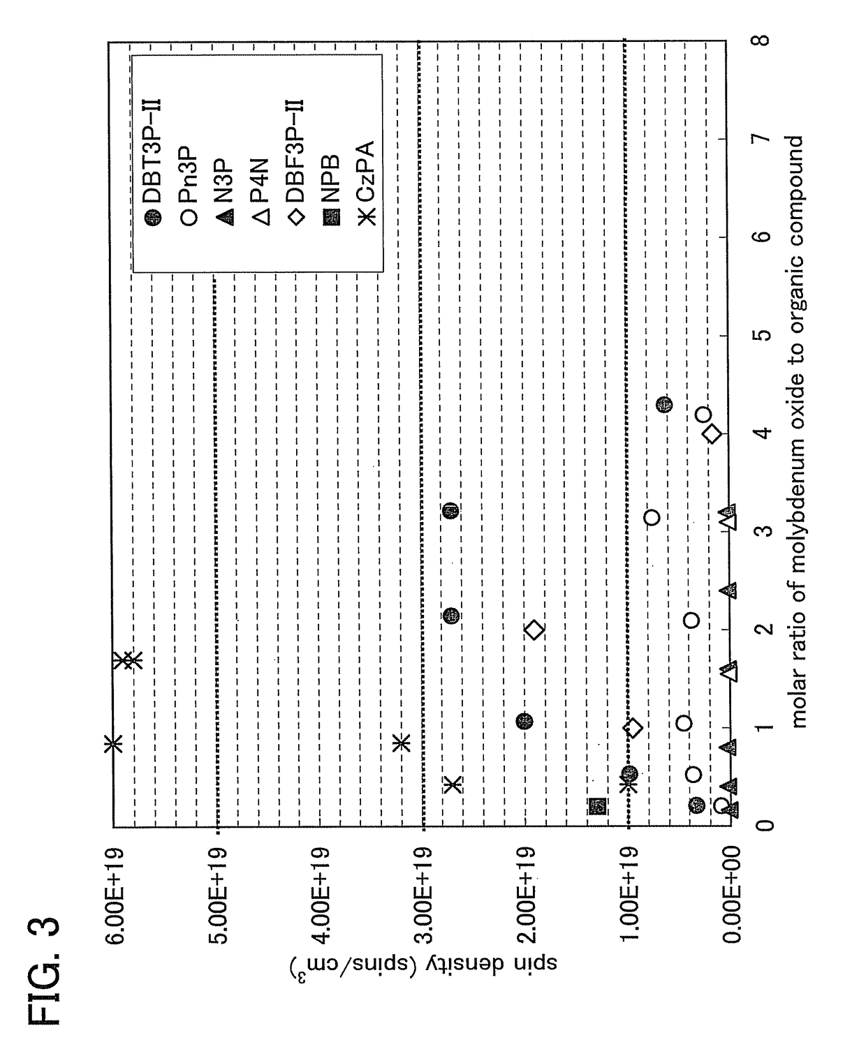
[0072]This embodiment shows results of the evaluation of composite materials each including an organic compound having a high hole-transport property and an electron acceptor, using an ESR method.

[0073]Samples used for the measurements are described below. All the samples were formed by co-evaporation of an organic compound and an electron acceptor over a quartz substrate having a size of 2.8 mm×20 mm, so that layers formed by the co-evaporation each contained the composite material including the organic compound and the electron acceptor.

[0074]The way how the samples were formed is specifically as follows. First, the quartz substrate was fixed to a holder in a vacuum evaporation apparatus so that a surface over which the composite material was to be formed by evaporation faced downward. After the pressure in the vacuum evaporation apparatus was reduced to 10−4 Pa, the organic compound and molybdenum(VI) oxide, which was an electron acceptor, were co-evaporated, thereby forming a la...

embodiment 3

[0092]In this embodiment, a layer containing a composite material which includes an organic compound having a high hole-transport property and an electron acceptor and in which charge-transfer interaction does not occur easily is provided in contact with the cathode 102 in the EL layer 103.

[0093]FIG. 4 illustrates a structure example of the light-emitting element in accordance with one embodiment of the present invention. The light-emitting element illustrated in FIG. 4 includes an anode 101 and a cathode 102, which correspond to the pair of electrodes, and an EL layer 103 provided between the anode 101 and the cathode 102.

[0094]In the example in FIG. 4, the EL layer 103 includes a charge generation layer 110 in addition to the hole-injection layer 104, the hole-transport layer 105, the light-emitting layer 106, the electron-transport layer 107, the electron-injection layer 108, and the like. Specifically, the hole-injection layer 104, the hole-transport layer 105, the light-emittin...


PUM


Abstract

Provided are a light-emitting element capable of reducing power consumption by increasing its light extraction efficiency and a light-emitting device using the light-emitting element. A light-emitting element includes a composite material, which contains an organic compound having a high hole-transport property and an electron acceptor and in which the spin density measured by an electron spin resonance (ESR) method is less than or equal to 1×10¹⁹ spins / cm3, the spin density is less than or equal to 3×10¹⁹ spins / cm3 when the molar ratio of the electron acceptor to the organic compound is greater than or equal to 1, or the spin density is less than or equal to 5×10¹⁹ spins / cm3 when the molar ratio is greater than or equal to 2.

Description

BACKGROUND OF THE INVENTION[0001]1. Field of the Invention[0002]The present invention relates to a light-emitting element having an EL layer between a pair of electrodes. Further, the present invention relates to a light-emitting device using the light-emitting element.[0003]2. Description of the Related Art[0004]Since light-emitting elements having an EL layer between a pair of electrodes are self-emission elements, high visibility can be achieved, they can be suitably used for thinner devices in that backlights needed for liquid crystal display devices (LCDs) are unnecessary, and the viewing angle has no limits. Thus, display devices using light-emitting elements have attracted attention as an alternative to CRTs or LCDs and have been increasingly put into practical use. Furthermore, light-emitting elements are thin planar light sources, and fewer limitations are imposed on their shapes. Thus, lighting devices having light-emitting elements as light sources have been expected to f...

Claims


Application Information

Patent Timeline
Patent Type & Authority Patents(United States)
IPC IPC(8): H01L51/54H01L51/50H01L51/52
CPCH01L51/506H01L51/5278H01L2251/55H10K50/155H10K50/19H10K2101/00H01L2924/01042H01L2924/01023H01L2924/01074H10K50/15H10K50/16
Inventor SEO, HIROMISEO, SATOSHI
Owner SEMICON ENERGY LAB CO LTD
Why Eureka
Try Eureka