High voltage electromagnetic induction device

a high-voltage electromagnetic and induction device technology, applied in the direction of transformer/inductance casing, basic electric elements, electrical equipment, etc., can solve the problems of increasing the maximum stress, the electric resistance in the longitudinal direction along the duct increases closer, and the lead-through device surface has a drawback, etc., to reduce the maximum stress, reduce the diameter, and reduce the effect of electric withstand strength

Active Publication Date: 2017-06-06
HITACHI ENERGY LTD
View PDF4 Cites 0 Cited by
  • Summary
  • Abstract
  • Description
  • Claims
  • Application Information

AI Technical Summary

Benefits of technology

[0006]The inventors of the present disclosure have realised that the lead-through device surface has a drawback in that the electric resistance in the longitudinal direction along the duct increases closer to the lead-through device end. The reason for that is that the cross-sectional area between the barrier and the lead-through device is smaller compared to solutions which have a number of cylindrical barriers arranged around the lead-through device end portion, due to the reduced diameter provided by the barrier. An uneven resistance distribution results in uneven stress and creep stress distribution which naturally results in increased maximum stresses and therefore reduced electric withstand strength.
[0009]An effect which may be obtainable by means of the different angles of the tapering internal portion of the bushing and the electrical insulation barrier, in particular by means of an increasing distance between the bushing and the electrical insulation barrier the further away from the opening, is that the electrical field may be controlled in a more beneficial manner. In particular, a more even voltage drop, stress and creep stress may be obtained.

Problems solved by technology

The inventors of the present disclosure have realised that the lead-through device surface has a drawback in that the electric resistance in the longitudinal direction along the duct increases closer to the lead-through device end.
An uneven resistance distribution results in uneven stress and creep stress distribution which naturally results in increased maximum stresses and therefore reduced electric withstand strength.

Method used


Image

  • High voltage electromagnetic induction device
  • High voltage electromagnetic induction device
  • High voltage electromagnetic induction device

Examples


Embodiment Construction

[0028]The inventive concept will now be described more fully hereinafter with reference to the accompanying drawings, in which exemplifying embodiments are shown. The inventive concept may, however, be embodied in many different forms and should not be construed as limited to the embodiments set forth herein; rather, these embodiments are provided by way of example so that this disclosure will be thorough and complete, and will fully convey the scope of the inventive concept to those skilled in the art. Like numbers refer to like elements throughout the description.

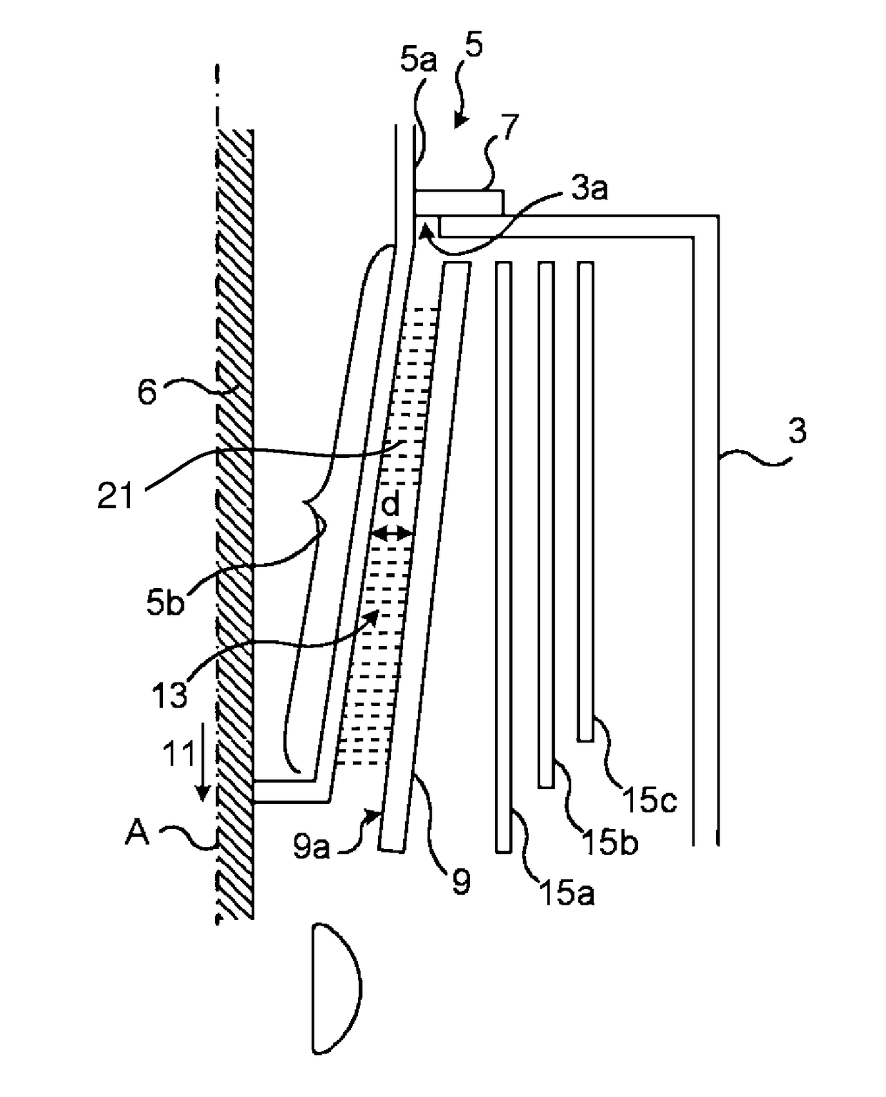
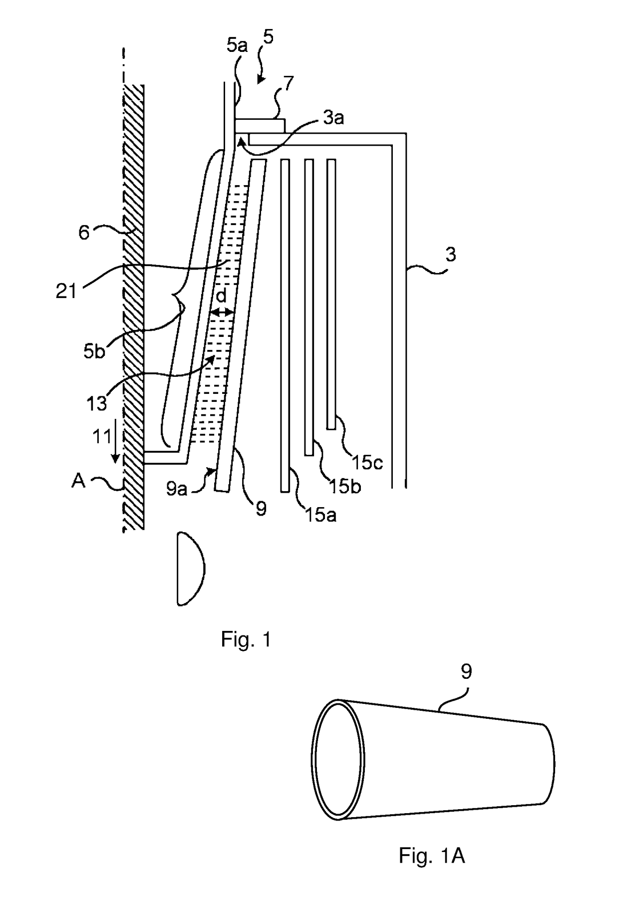
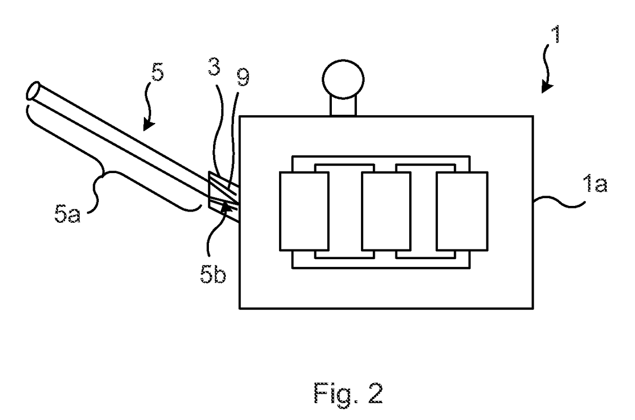
[0029]FIG. 1 shows a portion of a high voltage electromagnetic induction device 1 depicted in FIG. 2. The high voltage electromagnetic induction device 1 comprises a lead-through device-receiving structure 3 which has an opening 3a arranged to receive a lead-through device. The lead-through device-receiving structure 3 thus defines a means through which a lead-through device can be lead into the high voltage electromagnet...


PUM

PropertyMeasurementUnit
voltageaaaaaaaaaa
distanceaaaaaaaaaa
tapering angleaaaaaaaaaa

Abstract

A high voltage electromagnetic induction device including: a lead-through device-receiving structure having an opening for receiving a lead-through device, a lead-through device extending through the opening, wherein an internal portion is tapering in a direction along the central axis of the lead-through device away from the opening, and an electrical insulation barrier which is arranged in the lead-through device-receiving structure, arranged around and distanced from the internal portion, and which electrical insulation barrier is tapering in the direction, whereby a duct is formed between the internal surface of the electrical insulation barrier and the external surface of the internal portion of the lead-through device, wherein the electrical insulation barrier is tapering relative to the lead-through device such that the distance between the internal surface of the electrical insulation barrier and the external surface of the lead-through device increases in the direction.

Description

FIELD OF THE INVENTION[0001]The present disclosure generally relates to high voltage electromagnetic induction devices. In particular it relates to a high voltage electromagnetic induction device which comprises a lead-through device and an electrical insulation barrier arranged to insulate the lead-through device within the high voltage electromagnetic induction device.BACKGROUND OF THE INVENTION[0002]A high voltage electromagnetic induction device, such as a power transformer or a reactor, typically comprises a lead-through device which is an electrically insulated elongated device having a conductor arranged along its central axis.[0003]The lead-through device extends into the high voltage electromagnetic induction device through a wall of the high voltage electromagnetic induction device and connects with the internal electric components. The lead-through device thus provides electrical insulation between the conductor and the wall, which typically has a significantly different ...

Claims


Application Information

Patent Timeline
Patent Type & Authority Patents(United States)
IPC IPC(8): H02G3/18H01B17/28H01B17/26H01F27/04H01F27/02
CPCH01F27/04H01F27/022
Inventor ERIKSSON, ANDERSWEDIN, ERIKLINDGREN, JANBERGLUND, MATSRAMKVIST, MATSBERTILSSON, STINABRUNSTROM, TINA
Owner HITACHI ENERGY LTD
Why Eureka
Try Eureka