Semiconductor structure and process for forming plug including layer with pulled back sidewall part

a technology of semiconductor and plug, which is applied in the direction of semiconductor devices, semiconductor/solid-state device details, electrical apparatus, etc., to achieve the effect of improving the forming of the plug and increasing the opening of the recess

Active Publication Date: 2017-06-13
UNITED MICROELECTRONICS CORP
View PDF4 Cites 7 Cited by
  • Summary
  • Abstract
  • Description
  • Claims
  • Application Information

AI Technical Summary

Benefits of technology

[0005]The present invention provides a semiconductor structure and process for forming a plug, which pulls back layers formed in the plug to improve gap filling capability.
[0008]According to the above, the present invention provides a semiconductor structure and process for forming a plug, which forms a recess in a dielectric layer; sequentially covers a titanium layer and a first titanium nitride layer in the recess; pulls back the first titanium nitride layer; and then, covers a second titanium nitride layer in the recess, the titanium layer and the first titanium nitride layer. Due to the first titanium nitride layer being pulled back, the opening of the recess can be increased, and thus gap filling capability for forming the plug can be improved.

Problems solved by technology

As the miniaturization of semiconductor devices increases, filling the barrier layer and the low resistivity into a contact hole has become an important issue to form the contact plug and maintaining or enhancing the performances of formed semiconductor devices as well.

Method used


Image

  • Semiconductor structure and process for forming plug including layer with pulled back sidewall part
  • Semiconductor structure and process for forming plug including layer with pulled back sidewall part
  • Semiconductor structure and process for forming plug including layer with pulled back sidewall part

Examples


Embodiment Construction

[0012]The present invention is applied in a planar transistor in this embodiment, but the present invention can also be applied in a non-planar transistor such as a multi-gate MOSFET, depending upon practical requirements.

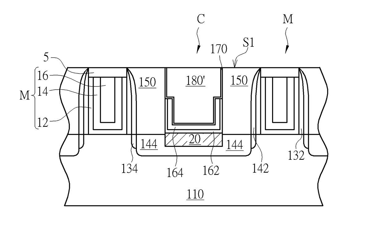
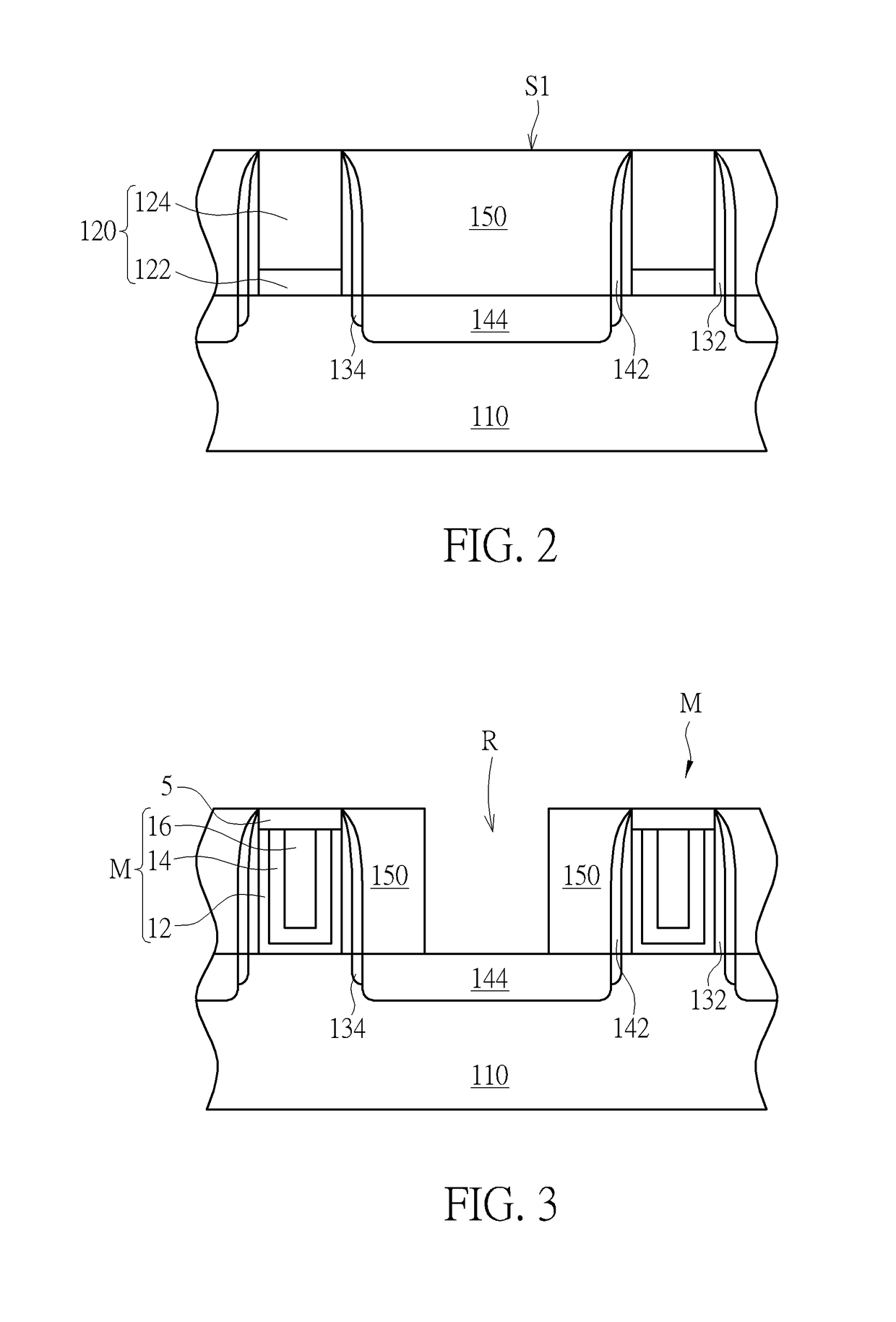
[0013]FIG. 1 schematically depicts a flow chart of a semiconductor process for forming a plug according to an embodiment of the present invention. FIGS. 2-10 schematically depict cross-sectional views of a semiconductor process for forming a plug according to an embodiment of the present invention. Please refer to a flowchart of the present invention in FIG. 1 and the corresponding cross-sectional views of the present invention in FIGS. 2-10 at the same time.

[0014]According to step S1 of FIG. 1—forming a dielectric layer having a recess on a substrate, please refer to FIGS. 2-3. As shown in FIG. 2, a substrate 110 is provided. The substrate 110 may be a semiconductor substrate such as a silicon substrate, a silicon containing substrate, a III-V group-on-silicon (su...


PUM

PropertyMeasurementUnit
dielectric constantaaaaaaaaaa
thicknesses k2aaaaaaaaaa

Abstract

A semiconductor process for forming a plug includes the following steps. A dielectric layer having a recess is formed on a substrate. A titanium layer is formed to conformally cover the recess. A first titanium nitride layer is formed to conformally cover the titanium layer, thereby the first titanium nitride layer having first sidewall parts. The first sidewall parts of the first titanium nitride layer are pulled back, thereby second sidewall parts being formed. A second titanium nitride layer is formed to cover the recess. Moreover, a semiconductor structure formed by said semiconductor process is also provided.

Description

BACKGROUND OF THE INVENTION[0001]1. Field of the Invention[0002]The present invention relates generally to a semiconductor structure and process for forming a plug, and more specifically to a semiconductor structure and process applying a layers-pulling back process for forming a plug.[0003]2. Description of the Prior Art[0004]Field effect transistors are important electronic devices in the fabrication of integrated circuits, and as the size of the semiconductor device becomes smaller and smaller, the fabrication of the transistors also improves and is constantly enhanced for fabricating transistors with smaller sizes and higher quality. In the conventional method of fabricating transistors, agate structure is first formed on a substrate, and a lightly doped drain (LDD) is formed on the two corresponding sides of the gate structure. Next, a spacer is formed on the sidewall of the gate structure and an ion implantation process is performed to forma source / drain region within the subs...

Claims


Application Information

Patent Timeline
Patent Type & Authority Patents(United States)
IPC IPC(8): H01L23/48H01L23/485H01L21/768H01L23/532
CPCH01L21/76895H01L21/76805H01L21/76846H01L21/76889H01L23/485H01L23/53238H01L23/53266H01L21/76897H01L21/28518H01L21/76855H01L21/76865H01L21/28568H01L21/76802H01L21/76849H01L21/76877
Inventor CHEN, PIN-HONGLAI, KUO-CHIHHSU, CHIA CHANGCHIU, CHUN-CHIEHCHEN, LI-HANHUANG, SHU MINTSAI, MIN-CHUANHUANG, HSIN-FUHSU, CHI-MAO
Owner UNITED MICROELECTRONICS CORP
Why Eureka
Try Eureka