Method of forming isolation structure

a technology of isolation structure and isolation structure, which is applied in the direction of semiconductor/solid-state device manufacturing, basic electric elements, electric apparatus, etc., can solve the problems of decreasing distances and arrangements between devices within semiconductor substrates, and becoming more tight, so as to avoid uneven stresses

Active Publication Date: 2020-03-05
UNITED MICROELECTRONICS CORP +1
View PDF0 Cites 2 Cited by
  • Summary
  • Abstract
  • Description
  • Claims
  • Application Information

AI Technical Summary

Benefits of technology

[0003]The present invention provides a method of forming an isolation structure, which fills up recesses with an oxide layer formed by an in-situ steam generation (ISSG) process, and thus gap filling capability can be improved and uneven stresses can be avoided.

Problems solved by technology

Due to integrated circuit devices evolving to be smaller and smaller and an increase of integration, distances and arrangements between devices within a semiconductor substrate are decreasing and becoming more tight.

Method used


Image

  • Method of forming isolation structure
  • Method of forming isolation structure
  • Method of forming isolation structure

Examples


Embodiment Construction

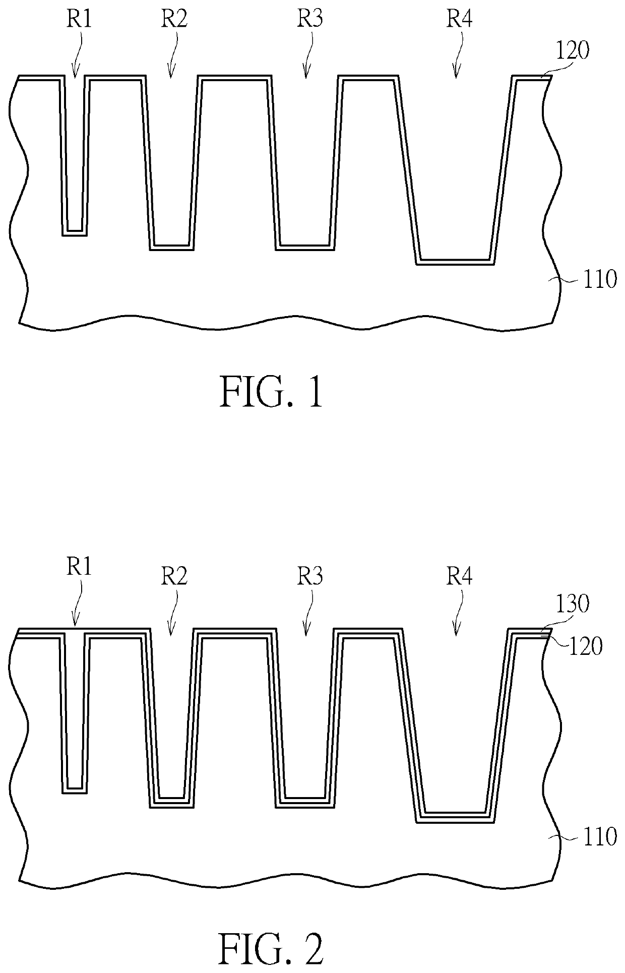
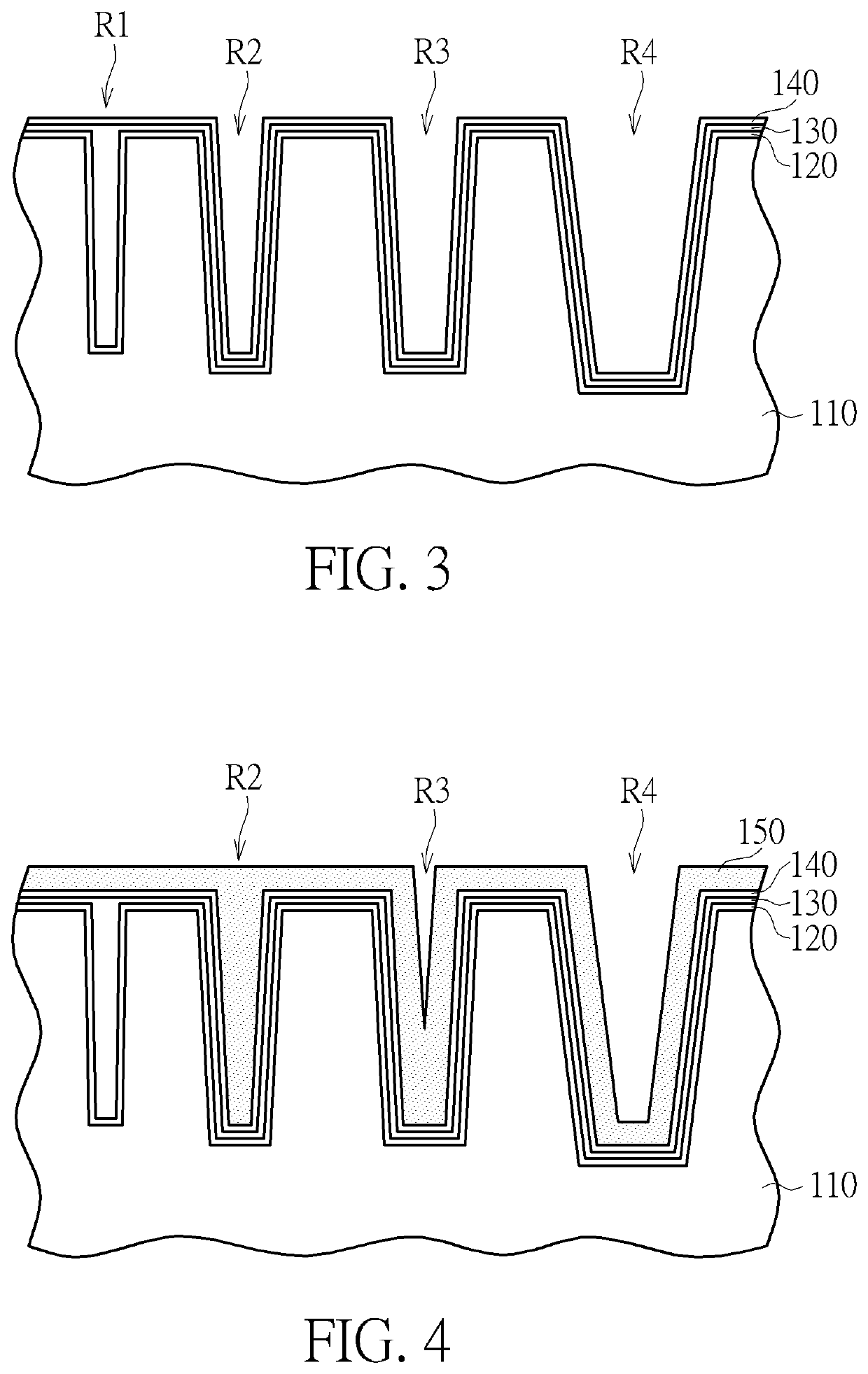
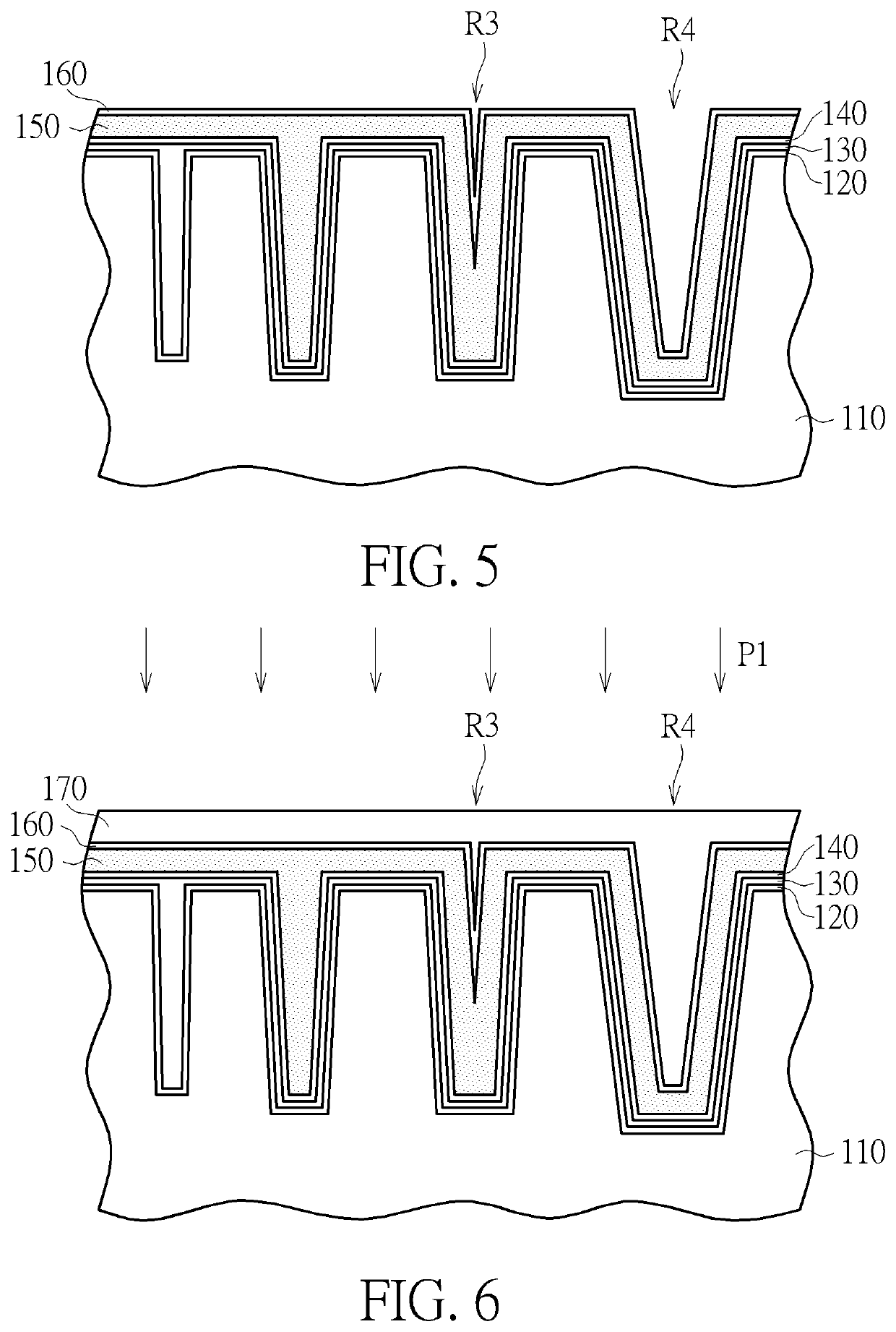
[0020]FIGS. 1-8 schematically depict cross-sectional views of a method of forming an isolation structure according to an embodiment of the present invention. As shown in FIG. 1, a substrate 110 is provided. The substrate 110 may be a semiconductor substrate such as a silicon substrate, a silicon containing substrate, a III-V group-on-silicon (such as GaN-on-silicon) substrate, a graphene-on-silicon substrate or a silicon-on-insulator (SOI) substrate. Recesses R1 / R2 / R3 / R4 are formed in the substrate 110, wherein the opening of the recess R4 is larger than the opening of the recess R3, the opening of the recess R3 is larger than the opening of the recess R2, and the opening of the recess R2 is larger than the opening of the recess R1. Methods of forming the recesses R1 / R2 / R3 / R4 may include the following steps. A hard mask layer (not shown) blanketly covers the substrate 110, the hard mask layer is patterned to expose a part of the substrate 110 for forming the recesses R1 / R2 / R3 / R4, th...


PUM

PropertyMeasurementUnit
processing temperatureaaaaaaaaaa
thicknessaaaaaaaaaa

Abstract

A method of forming an isolation structure includes the following steps. A substrate having a first trench, a second trench and a third trench is provided, wherein the opening of the third trench is larger than the opening of the second trench, and the opening of the second trench is larger than the opening of the first trench. A first oxide layer is formed to conformally cover the first trench, the second trench and the third trench by an atomic layer deposition (ALD) process. A second oxide layer fills up the first trench by an in-situ steam generation (ISSG) process.

Description

BACKGROUND OF THE INVENTION1. Field of the Invention[0001]The present invention relates generally to a method of forming an isolation structure, and more specifically to a method of forming an isolation structure applying an in-situ steam generation (ISSG) process to fill up recesses.2. Description of the Prior Art[0002]Due to integrated circuit devices evolving to be smaller and smaller and an increase of integration, distances and arrangements between devices within a semiconductor substrate are decreasing and becoming more tight. Therefore, suitable insulating or isolation has to be formed between each device to prevent each device from junction current leakage, and an insulating or isolation region is reduced to enhance integration in a perfect isolation. In various device isolation technologies, localized oxidation isolation (LOCOS) and shallow trench isolation (STI) are the most often used. In particular, STI has advantages of a smaller isolation region and retaining planariza...

Claims


Application Information

Patent Timeline
Patent Type & Authority Applications(United States)
IPC IPC(8): H01L21/762H01L21/02
CPCH01L21/02554H01L21/76224H01L21/0254H01L21/0228H01L21/76229
Inventor CHEN, PO-CHUNCHU, HSUAN-TUNGCHEN, YI-WEILIU, WEI-HSINTUNG, YU-CHENGCHANG, CHIA-LUNG
Owner UNITED MICROELECTRONICS CORP
Why Eureka
Try Eureka