

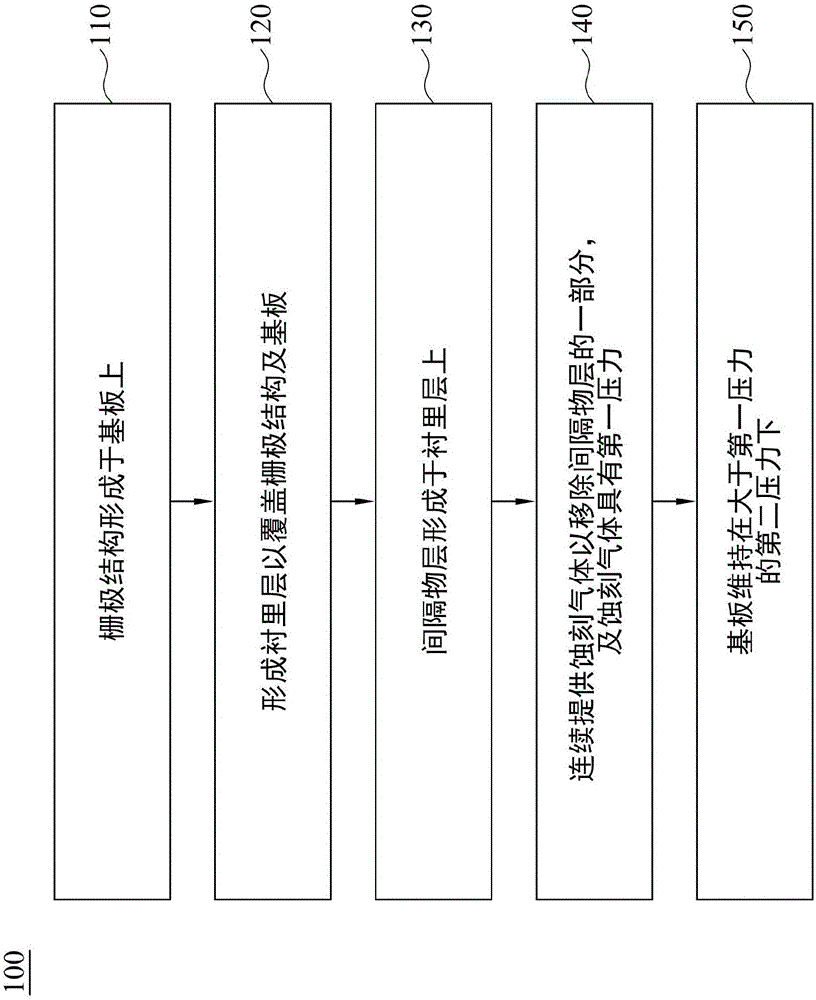
Method of fabricating semiconductor structure
A technology of conductor structure and gate structure, which is applied in the direction of semiconductor devices, semiconductor/solid-state device manufacturing, transistors, etc., and can solve the problems of increasing the complexity of the integrated circuit manufacturing process.
- Summary
- Abstract
- Description
- Claims
- Application Information
AI Technical Summary
Problems solved by technology
Method used
Image

Examples
Embodiment Construction
[0012] The following disclosure provides numerous different embodiments or examples for implementing different features of the subject matter provided herein. Specific examples of components and arrangements are described below to simplify the present disclosure. Such components and arrangements are of course examples only and are not intended to be limiting. For example, in the description below, the formation of a first feature on or over a second feature may include embodiments in which the first feature is formed in direct contact with the second feature, and may also include embodiments in which the first feature is formed in direct contact with the second feature. Embodiments where additional features are formed between second features such that the first and second features are not in direct contact. In addition, the present invention may repeat element symbols and / or letters in various examples. This repetition is for purposes of simplicity and clarity, and does not ...
PUM
 Abstract
Description
Claims
Application Information