Supercharge Your Innovation With Domain-Expert AI Agents!

Optoelectronic component with organic and inorganic charge generating layers and method for producing an optoelectronic component

a technology of organic and inorganic charge generation and optoelectronic components, which is applied in the direction of solid-state devices, organic semiconductor devices, semiconductor devices, etc., can solve the problems of reducing the efficiency of stacked oleds, limiting the operating period of organic optoelectronic components, and inability to use drop for light generation

Active Publication Date: 2017-06-20
DOLYA HOLDCO 5 LTD
View PDF28 Cites 4 Cited by
  • Summary
  • Abstract
  • Description
  • Claims
  • Application Information

AI Technical Summary

Benefits of technology

The patent text describes a method to create an optoelectronic component that can produce light. This component can be made using an organic material and is useful for creating displays or other lighting fixtures. The technical effects of this invention include providing an efficient and effective way to produce energy-efficient lighting that is durable and has a long lifespan.

Problems solved by technology

This voltage drop cannot be used for the generation of light and thus reduces the efficiency of the stacked OLEDs.
This limits the operating period of organic optoelectronic components.
A further disadvantage when using organic hole-conducting charge generating layer is the low charge carrier density thereof and the relatively weak interface dipoles.
The often weak interface dipoles make it more difficult to separate hole and electron at the interface of the hole-conducting charge generating layer and the first electron-conducting charge generating layer.
By means of the crystallization of the substance of the organic hole-conducting charge generating layers, the layer can lose its functionalities in the charge generating layer structure, such that the optoelectronic component can become unusable.
The formation of hole-conducting charge generating layers from inorganic substances has not been possible to be realized hitherto for a number of reasons.
In this regard, in the case of many known inorganic substances, the electrical properties are incompatible with the electrical properties of the organic first electron-conducting charge generating layer.
A further obstacle is presented by the generating conditions of the hole-conducting charge generating layer composed of an inorganic substance.
Inorganic substances for forming the hole-conducting charge generating layer are unsuitable if the hole-conducting charge generating layer can be formed only by production conditions which are incompatible with organic layers, e.g. temperature >>100° C.
What is furthermore disadvantageous in the choice of inorganic substances for the hole-conducting charge generating layer is the optical properties thereof, e.g. the transmission.

Method used


Image

  • Optoelectronic component with organic and inorganic charge generating layers and method for producing an optoelectronic component
  • Optoelectronic component with organic and inorganic charge generating layers and method for producing an optoelectronic component
  • Optoelectronic component with organic and inorganic charge generating layers and method for producing an optoelectronic component

Examples


Embodiment Construction

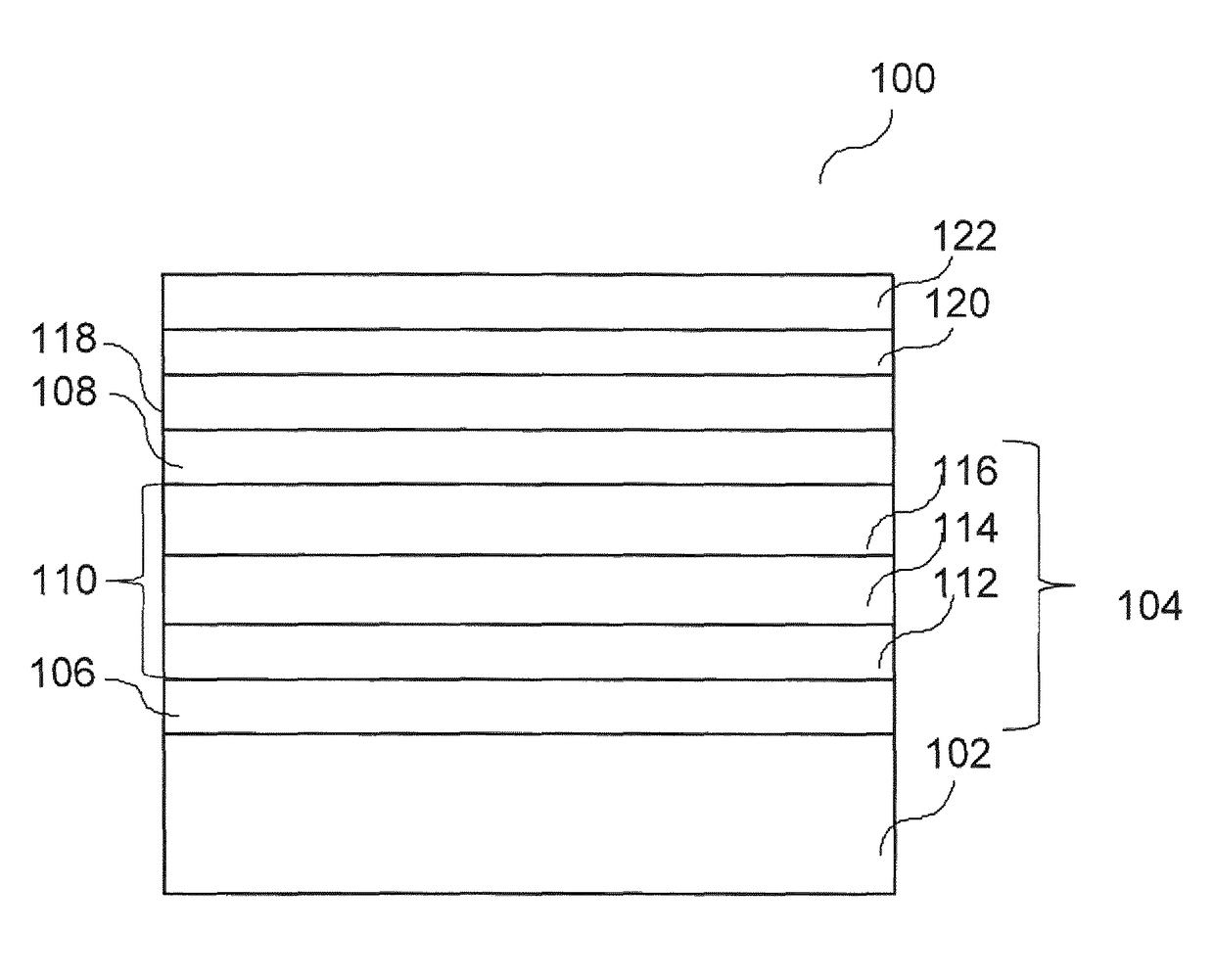
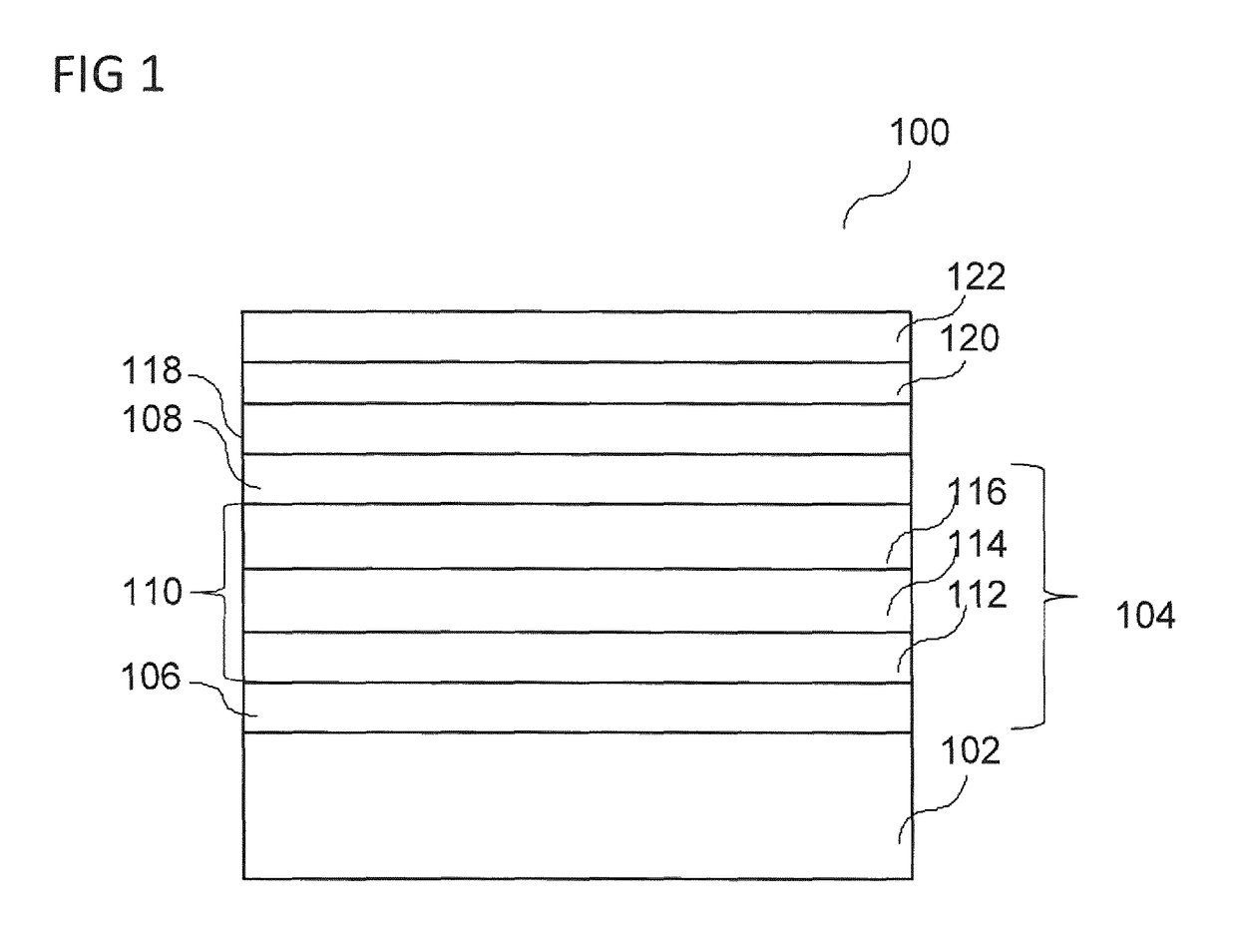
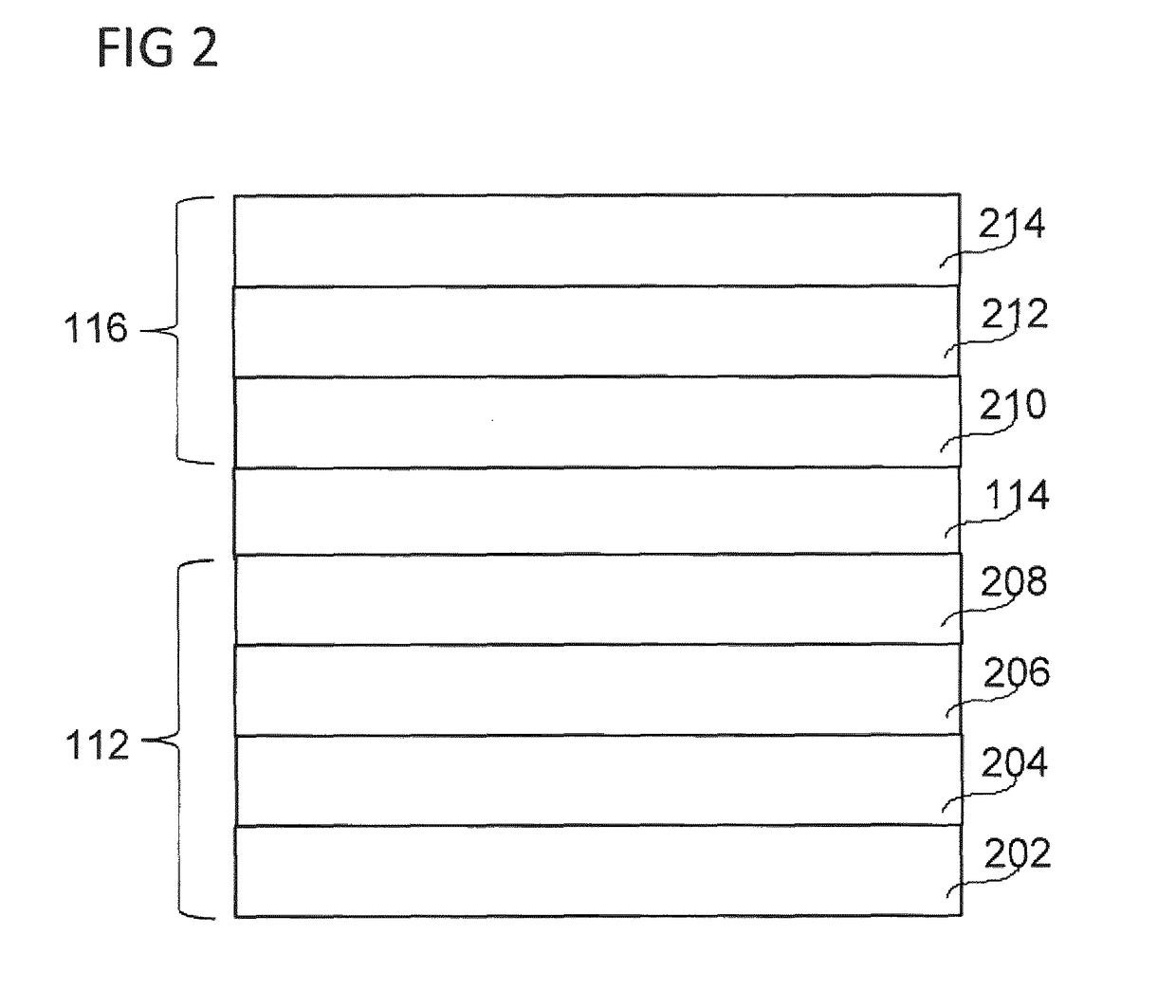
[0136]In the following detailed description, reference is made to the accompanying drawings, which form part of this description and show for illustration purposes specific embodiments in which the disclosure can be implemented. In this regard, direction terminology such as, for instance, “at the top”, “at the bottom”, “at the front”, “at the back”, “front”, “rear”, etc. is used with respect to the orientation of the figure(s) described. Since component parts of embodiments can be positioned in a number of different orientations, the direction terminology serves for illustration and is not restrictive in any way whatsoever. It goes without saying that other embodiments can be used and structural or logical changes can be made, without departing from the scope of protection of the present disclosure. It goes without saying that the features of the various embodiments described herein can be combined with one another, unless specifically indicated otherwise. Therefore, the following d...


PUM


Abstract

Various embodiments may relate to an optoelectronic component, including a first organic functional layer structure, a second organic functional layer structure and a charge generating layer structure between the first organic functional layer structure and the second organic functional layer structure. The charge generating layer structure includes a hole-conducting charge generating layer and a first electron-conducting charge generating layer. The hole-conducting charge generating layer includes or is formed from an inorganic substance or an inorganic substance mixture. The first electron-conducting charge generating layer includes or is formed from an organic substance or an organic substance mixture. The first electron-conducting charge generating layer includes or is formed from an organic, intrinsically electron-conducting substance.

Description

RELATED APPLICATIONS[0001]The present application is a national stage entry according to 35 U.S.C. §371 of PCT application No.: PCT / EP2013 / 063715 filed on Jun. 28, 2013, which claims priority from German application No. 10 2012 214 021.2 filed on Aug. 8, 2012, and is incorporated herein by reference in its entirety.TECHNICAL FIELD[0002]Various embodiments relate to an optoelectronic component and a method for producing an optoelectronic component.BACKGROUND[0003]An optoelectronic component (e.g. an organic light emitting diode (OLED), for example a white organic light emitting diode (WOLED), a solar cell, etc.) on an organic basis is usually distinguished by its mechanical flexibility and moderate production conditions. Compared with a component composed of inorganic materials, an optoelectronic component on an organic basis can be produced potentially cost-effectively on account of the possibility of large-area production methods (e.g. roll-to-roll production methods).[0004]A WOLED...

Claims


Application Information

Patent Timeline
Patent Type & Authority Patents(United States)
IPC IPC(8): H01L51/50H01L51/52H01L51/56H01L51/00H10K99/00
CPCH01L51/506H01L51/5008H01L51/508H01L51/5278H01L51/56H01L51/0072H01L2251/301H01L2251/303H10K50/19H10K71/00H10K71/30H10K50/155H10K30/865H10K50/166H10K85/6572H10K2102/00
Inventor REUSCH, THILODIEZ, CAROLA
Owner DOLYA HOLDCO 5 LTD
Features
  • R&D
  • Intellectual Property
  • Life Sciences
  • Materials
  • Tech Scout
  • Unparalleled Data Quality
  • Higher Quality Content
  • 60% Fewer Hallucinations
Learn More