Performance enhanced semiconductor socket

a technology of semiconductor sockets and sockets, applied in the direction of measurement devices, electrical measurement instrument details, instruments, etc., can solve the problems of reducing the space available for locating springs or contact members, ic sockets have reached mechanical and electrical limitations that require alternate methods, etc., to achieve reliable elastic deformation or compliance properties.

Active Publication Date: 2017-06-27
HSIO TECH
View PDF449 Cites 10 Cited by
  • Summary
  • Abstract
  • Description
  • Claims
  • Application Information

AI Technical Summary

Benefits of technology

[0013]The present disclosure is directed to an enhanced test socket with electrical and mechanical enhancements to address the challenges of next generation interconnect requirements. The present socket housing employs materials with varying dielectric constant and optional metallization in a selective manner to provide impedance tuning characteristics through the electrical path. The present test socket can use proven metallic contact members that provide reliable elastic deformation or compliance properties.
[0017]The present disclosure includes embodiments using spring probe style contact members because of their superior mechanical performance. At the same time, spring probe contact members also exhibit poor electrical performance due to the coil spring and the general metal structure. In one embodiment, a stack of drilled cores are assembled around the spring probe contact members in a compression mounted configuration, with the contact tips extending above and below the core surfaces to provide an electrical contact point between two mating circuits or packaged semiconductor devices. The stacked or layered socket housing reduces cost and permits the ability to mix and match the material stack based upon dielectric constant. Applicant has found that signal integrity of a spring probe contact member is greatly improved by varying the dielectric constant from layer to layer, the thickness of the layers, and the air gap around the contact member.

Problems solved by technology

As IC devices advance to next generation architectures traditional IC sockets have reached mechanical and electrical limitations that require alternate methods.
As the terminal pitch reduces, the available area to place a contact is also reduced, which limits the space available to locate a spring or contact member which can deflect without touching a neighbor.
In order to maximize the length of the spring so that it can deflect the proper amount without damage, the thickness of the insulating walls within the plastic housing is reduced which increases the difficulty of molding as well as the latent stress in the molded housing, resulting in warpage during the heat applied during solder reflow.
Long contact members tend to reduce the electrical performance of the connection by creating a parasitic effect that impacts the signal as it travels through the contact.
Other effects such as contact resistance impact the self-heating effects as current passes through power delivering contacts, and the small space between contacts can cause distortion as a nearby contact influences the neighbor which is known as cross talk.
Traditional socket methods are able to meet the mechanical compliance requirements of today's needs, but they have reached an electrical performance limit.
Next generation systems will operate above 5 GHz and beyond and the existing interconnects will not achieve acceptable performance levels without significant revision.
A major issue with the use of spring probes in test sockets is the electrical performance is degraded by the coil spring which is an inductor, as well as the potential capacitance of the metal members and the relatively high contact resistance due to the various sliding connection point.

Method used


Image

  • Performance enhanced semiconductor socket
  • Performance enhanced semiconductor socket
  • Performance enhanced semiconductor socket

Examples


Embodiment Construction

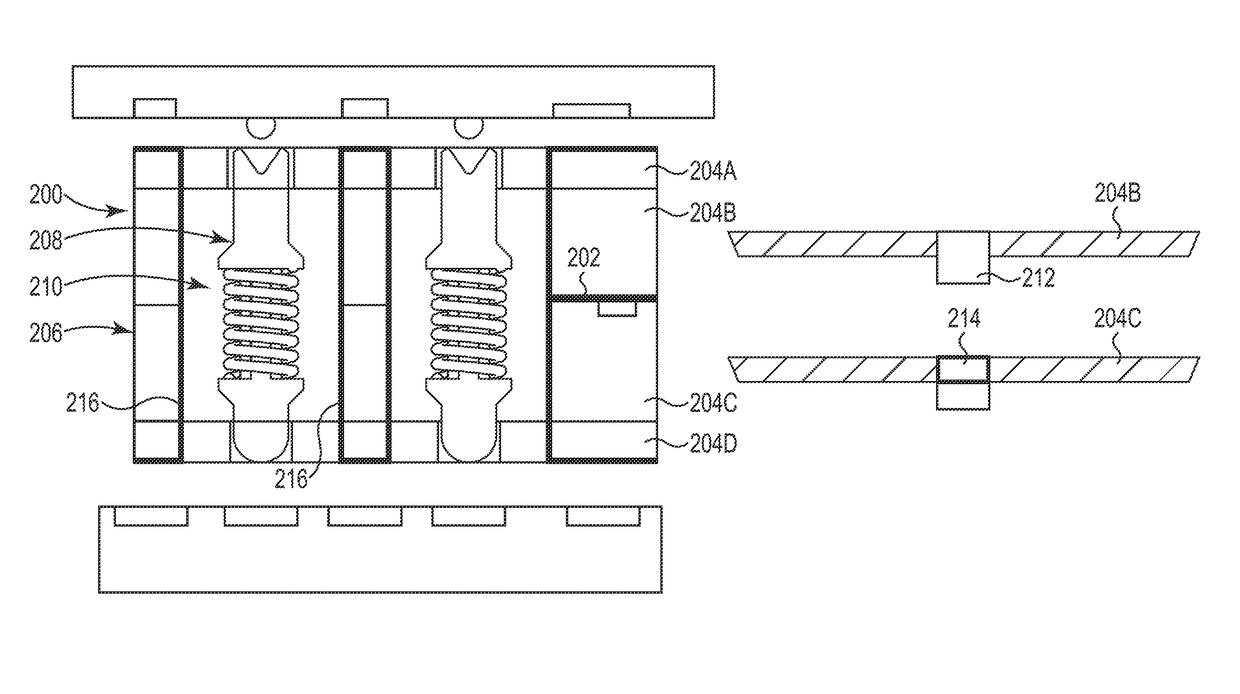
[0034]FIG. 1 is a sectional view of a test socket 50 with contact members 54 in accordance with an embodiment of the present disclosure. Socket housing 56 includes a plurality of openings 58 arranged to correspond with contacts 60 on integrated circuit device 62. In the illustrated embodiment, the contacts 60 are solder balls.

[0035]In the illustrated embodiment, the contact members 54 are spring contact members that provide superior mechanical performance in forming electrical connections with IC devices 62 and PCB 78. In one embodiment, shielding 52 surrounds the contact members 54. The spring contact members 54 are of a conventional structure with an upper portion 64 that slides axially relative to lower portion 66. Spring member 68 biases the upper portion 64 away from the lower portion 66 along axis 70. In application, upper portion 66 extends above top surface 72 of the socket housing 56 to engage with contact members 60 on the IC device 62. Simultaneously, lower portion 66 ext...


PUM

PropertyMeasurementUnit
dielectric constantsaaaaaaaaaa
dielectric constantaaaaaaaaaa

Abstract

A test socket for IC devices includes a multi-layered socket housing with at least one center layer and first and second surface layers. The first and second surface layers have a thickness and dielectric constant less than that of the center layers. A plurality of contact members are located in center openings in the center layer with distal ends extending into openings in the first and second layers. The distal ends of the contact members having at least one dimension greater than the openings in the first and second surface layers to retain the contact members in the socket housing. The contact members include center portions with major diameters less than the diameters of the center openings, such that an air gap is maintained between the contact members and the center layer.

Description

CROSS-REFERENCE TO RELATED APPLICATIONS[0001]This application claims the benefit of U.S. Provisional Application No. 61 / 914,179, filed Dec. 10, 2013, the disclosure of which is hereby incorporated by reference.[0002]The present application is a continuation-in-part of U.S. patent application Ser. No. 13 / 700,639, entitled Electrical Connector Insulator Housing, filed Nov. 28, 2012, which is a national stage application under 35 U.S.C. §371 of International Application No. PCT / US2011 / 038845, titled Electrical Connector Insulator Housing, filed Jun. 2, 2011, which claims the benefit of U.S. Provisional Application No. 61 / 351,114, entitled Electrical Connector Insulator Housing, filed Jun. 3, 2010, all of which are hereby incorporated by reference in their entireties.[0003]This application is a continuation-in-part of U.S. patent application Ser. No. 13 / 410,914, titled METALIZED PAD TO ELECTRICAL CONTACT INTERFACE, filed Mar. 2, 2012, which claims priority to U.S. Provisional Applicatio...

Claims


Application Information

Patent Timeline
Patent Type & Authority Patents(United States)
IPC IPC(8): G01R1/04
CPCG01R1/0466Y10T29/49222
Inventor RATHBURN, JAMES
Owner HSIO TECH
Why Eureka
Try Eureka