Method of making an electronic interconnect

a technology of electronic interconnection and assembly method, which is applied in the direction of coupling contact members, coupling device connections, printed circuit manufacturing, etc., can solve the problems of mechanical and electrical limitations, limiting the space available for positioning springs or contact members, and reducing the available area for placing contacts. , to achieve the effect of reliable flexural properties and reducing the complexity of contact members and tooling requirements

Active Publication Date: 2016-04-19
HSIO TECH
View PDF435 Cites 11 Cited by
  • Summary
  • Abstract
  • Description
  • Claims
  • Application Information

AI Technical Summary

Benefits of technology

[0015]The present disclosure relates to an electrical interconnect with metallic contact structures that provide reliable flexural properties. In one embodiment, the metallic contact structures mimic the mechanical details of a simple beam structure made of traditional materials, but removes the normal retention features that add parasitic mass and distort or degrade the integrity of the signal. The present disclosure provides a reliable connection to the package terminals and creates a platform to add electrical and mechanical enhancements to the socket substrate or assembly to address the challenges of next generation interconnect requirements. The lack of contact member retention features greatly reduces the complexity of the contact members and the tooling required to produce them.

Problems solved by technology

As systems advance to next generation architectures, these traditional have reached mechanical and electrical limitations that mandate alternate methods.
As the terminal pitch is reduced, the available area to place a contact is also reduced, which limits the space available to locate a spring or contact member which can deflect without touching an adjacent contact.
Long contact members, however, tend to reduce the electrical performance of the connection by creating a parasitic effect that impacts the signal as it travels through the contact.
Other effects such as contact resistance impact the self-heating effects as current passes through power delivering contacts, and the small space between contacts can cause distortion as a nearby contact influences the neighbor which is known as cross talk.
Traditional socket methods are able to meet the mechanical compliance requirements of today's needs, but they have reached an electrical performance limit.
Next generation systems will operate above 5 GHz and beyond and the existing interconnects will not achieve acceptable performance levels without significant revision.

Method used


Image

  • Method of making an electronic interconnect
  • Method of making an electronic interconnect
  • Method of making an electronic interconnect

Examples


Embodiment Construction

[0029]An electrical interconnect in accordance with the present disclosure permits fine contact-to-contact spacing (pitch) on the order of less than 1.0 millimeter (1×10⁻³ meter), and more preferably a pitch of less than about 0.7 millimeter, and most preferably a pitch of less than about 0.4 millimeter. Such fine pitch electrical interconnects are especially useful for communications, wireless, and memory devices. The disclosed low cost, high signal performance electrical interconnects, which have low profiles and can be soldered to the system PC board, are particularly useful for desktop and mobile PC applications.

[0030]The disclosed electrical interconnects permit IC devices to be installed and uninstalled without the need to reflow solder. The solder-free electrical connection of the IC devices is environmentally friendly.

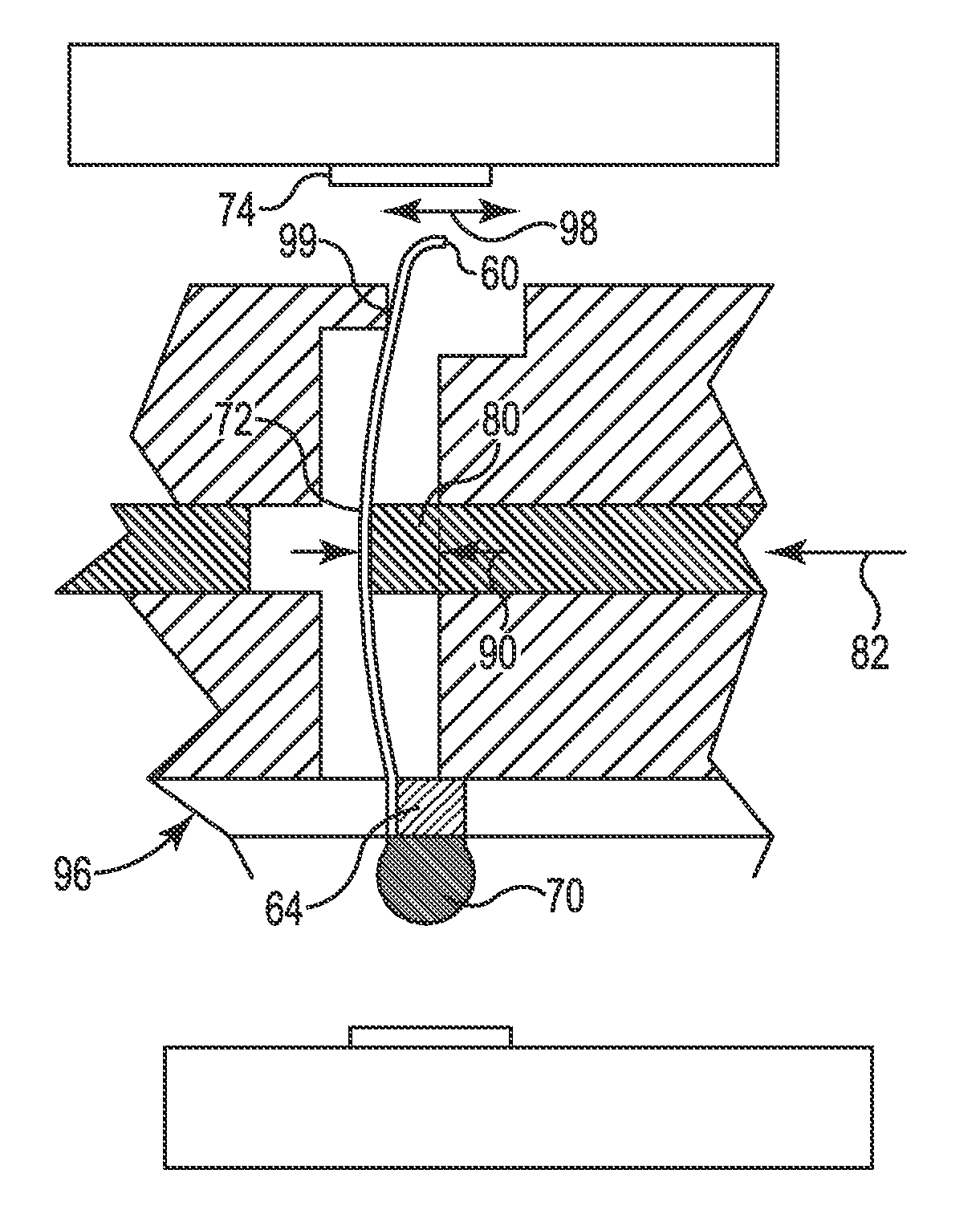
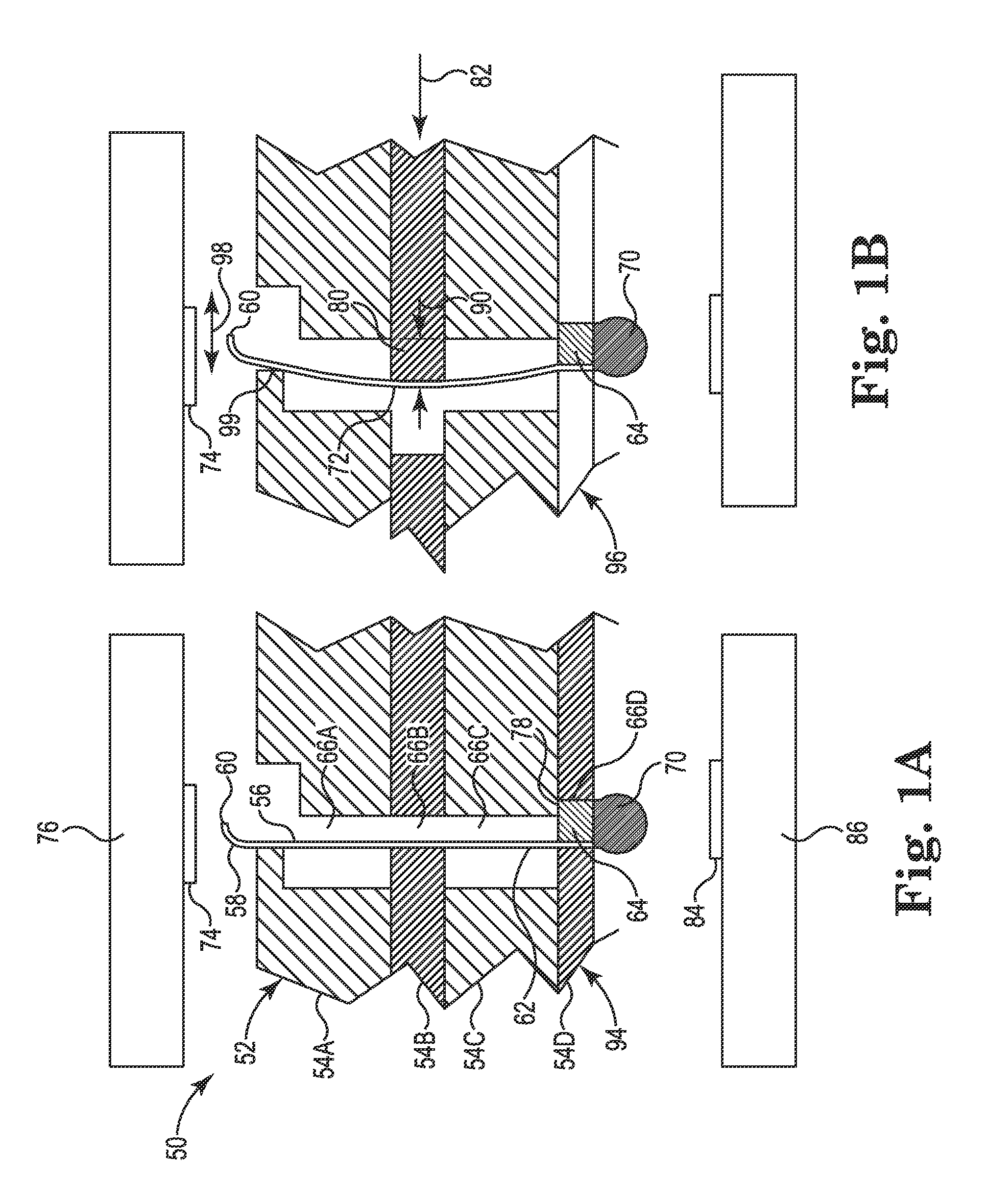
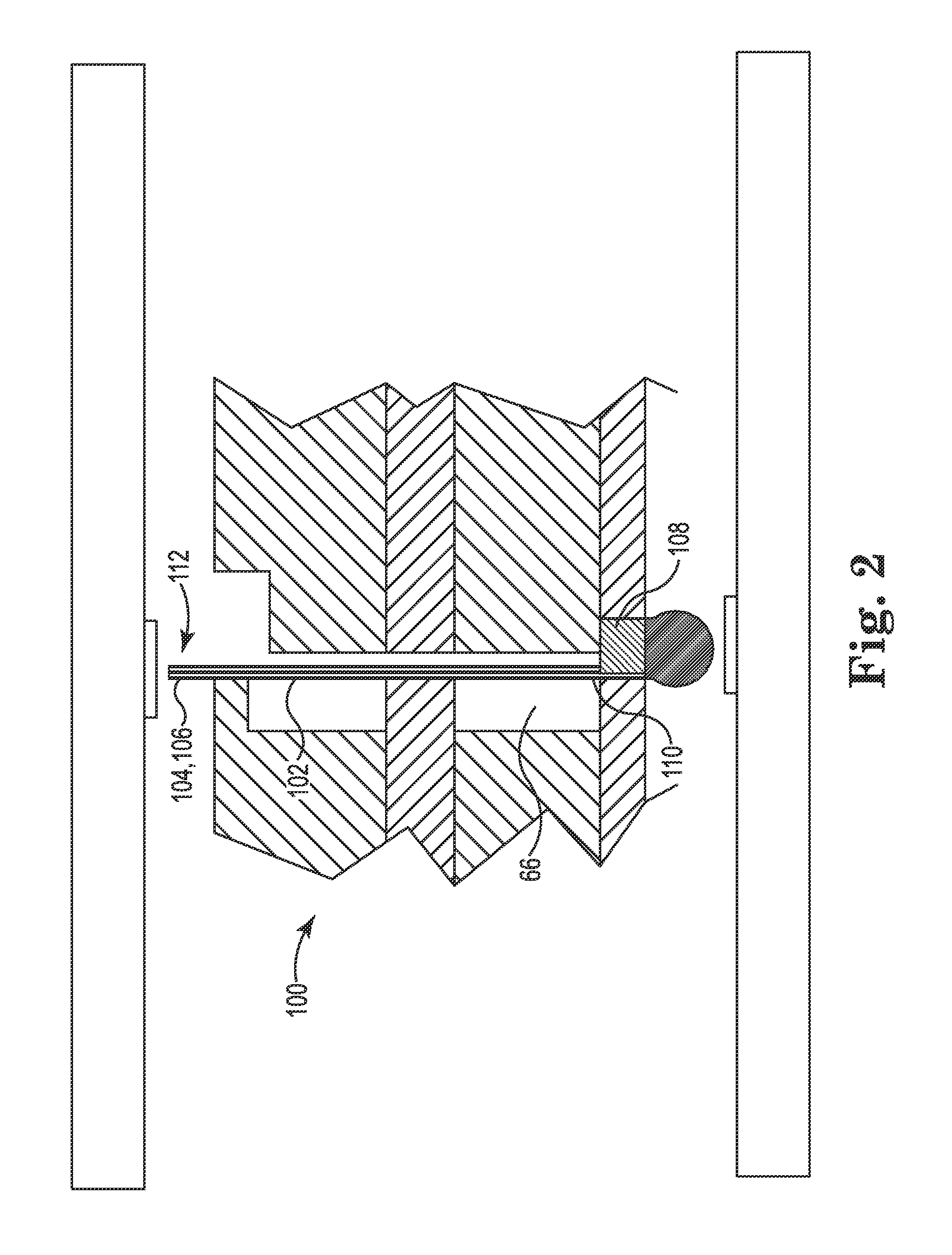
[0031]FIG. 1A is a side cross-sectional view of a portion of an electrical interconnect 50 in accordance with an embodiment of the present disclosure. Substrat...


PUM

PropertyMeasurementUnit
aspect ratioaaaaaaaaaa
conductiveaaaaaaaaaa

Abstract

An electrical interconnect including a substrate with at least two adjacent layers configured to translate relative to each other between a nominal position and a translated position. A plurality of through holes are formed through the layers from a first surface of the substrate to a second surface of the substrate in both the nominal position and the translated position. At least one contact member is positioned in the through holes with distal portions accessible from the first surface and a proximal portions positioned near the second surface. The proximal portion of the contact members are secured to the substrate near the second surface with a conductive structure. The two adjacent layers of the substrate are translated from the nominal position to the translated position to elastically deform the contact members within the through holes and to displace the distal portions of the contact members toward the conductive structures, respectively.

Description

RELATED APPLICATION[0001]This application claims the benefit of U.S. Provisional Application No. 61 / 812,455, filed Apr. 16, 2013, the disclosure of which is hereby incorporated by reference.[0002]This application is a continuation-in-part of U.S. patent application Ser. No. 13 / 320,285, entitled COMPLIANT PRINTED FLEXIBLE CIRCUIT, filed Nov. 14, 2011, which is a national stage application under 35 U.S.C. §371 of International Application No. PCT / US2010 / 036282, titled COMPLIANT PRINTED FLEXIBLE CIRCUIT, filed May 27, 2010, which claims priority to U.S. Provisional Application No. 61 / 183,340, filed Jun. 2, 2009, both of which are hereby incorporated by reference in their entireties.[0003]This application is a continuation-in-part of U.S. patent application Ser. No. 13 / 318,369, entitled COMPOSITE POLYMER-METAL ELECTRICAL CONTACT filed Nov. 1, 2011, which is a national stage application under 35 U.S.C. §371 of International Application No. PCT / US2010 / 036295, titled COMPOSITE POLYMER-META...

Claims


Application Information

Patent Timeline
Patent Type & Authority Patents(United States)
IPC IPC(8): H05K3/00H05K3/02H01R43/18H01R12/71H01R13/24H01R13/193H01R13/436
CPCH01R43/18H01R12/714H01R13/2442H01R13/193H01R13/4361Y10T29/49155
Inventor RATHBURN, JIM
Owner HSIO TECH
Why Eureka
Try Eureka