Fiber optical superconducting nanowire single photon detector

a fiber optical and nanowire technology, applied in the field of low-level light detectors, can solve the problems of low detection efficiency, low coupling efficiency, and low detection efficiency of either system, and achieve the effects of increasing detector efficiency, precise alignment of detectors, and maximizing coupling efficiency

Active Publication Date: 2017-08-08
TECHNION RES & DEV FOUND LTD
View PDF31 Cites 9 Cited by
  • Summary
  • Abstract
  • Description
  • Claims
  • Application Information

AI Technical Summary

Benefits of technology

[0011]The present disclosure describes new exemplary light detection devices, especially using SNSPD detection elements, having novel configurations for increasing the detector efficiency. Firstly, the detector is fabricated directly on the tip of an optical fiber used for inputting the light. The fabrication on the tip of the fiber allows precise alignment of the detector to the fiber core, where the field mode is maximal. This construction maximizes the coupling efficiency ηC to close to unity, without the need for complex alignment procedures, as is necessary with prior art devices in which the input fiber is brought into proximity and aligned with a previously fabricated device.
[0012]Additionally, the device can be constructed to include a high-Q optical cavity, such that any photon entering the device will be reflected to and fro within the cavity numerous times. This is achieved by ensuring that both end reflectors of the resonant optical cavity are mirrors having as high a reflectivity as possible. This construction is achieved by incorporating dedicated mirrors at both ends of the cavity, rather than using the nanowire structure itself, or a reflective coating on it, as one of the cavity mirrors, which is the configuration shown in at least some of the prior art. The cavity is thus characterized in that the meander nanowire structure is contained within the cavity between the end mirrors. Therefore, the above mentioned effect of photons being reflected to and fro within the cavity numerous times, and traversing the meander nanowire structure at every pass, thus results in their having greatly increased chances of absorption by the nanowire structure.

Problems solved by technology

This results in the formation of a localized non-superconducting region, or hotspot, with finite electrical resistance.
Current SNSPDs can thus provide fast response, as well as negligible dark counts, but suffer from detection efficiencies well below 100%.
Either of these systems is complex, costly, and slow to operate.
These methods may result is light losses of the order of 50% or more.
Moreover, the light is not generally confined in the directions perpendicular to the beam propagation direction, which result in light loss to the sides.
Furthermore, the above described prior art devices still require a sensitive and time consuming alignment procedure to ensure that the light input fall entirely on the SNSPD element.

Method used


Image

  • Fiber optical superconducting nanowire single photon detector
  • Fiber optical superconducting nanowire single photon detector
  • Fiber optical superconducting nanowire single photon detector

Examples


Embodiment Construction

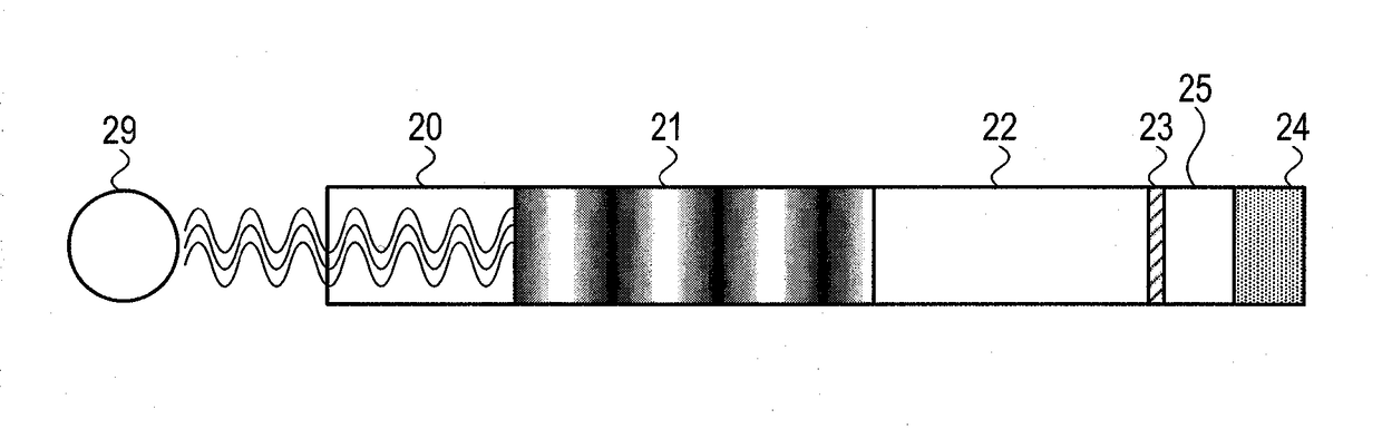
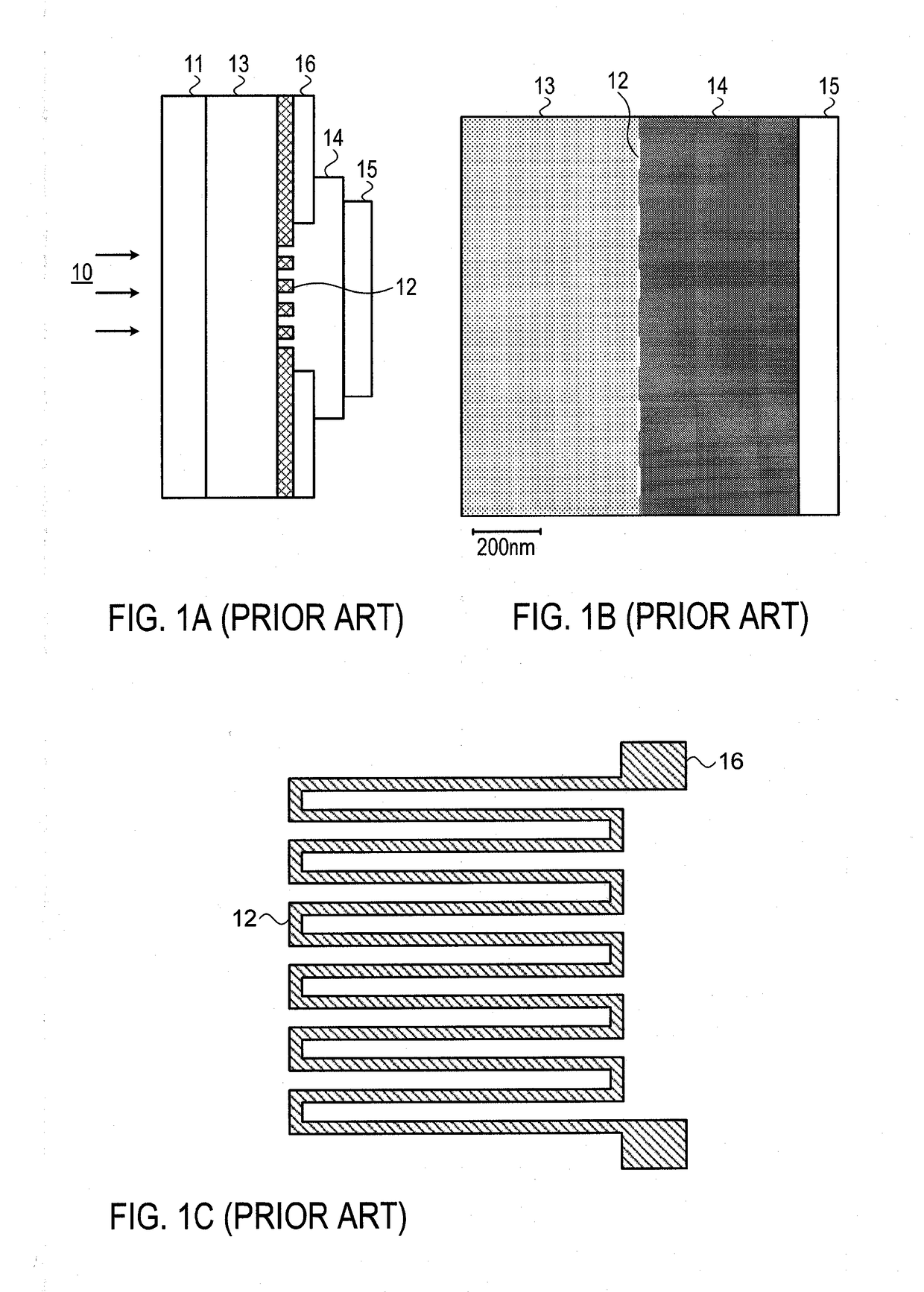
[0037]Reference is now made to FIGS. 1A, 1B and 1C, which illustrate schematically a prior art SNSPD, of the type shown in the above referenced article entitled “Nanowire Single Photon Detector with an Integrated Optical Cavity and Antireflection Coating” by K. M. Rosfjord et al, published in Optics Express, Vol. 14, No. 2, pp. 527-534 (2006). FIG. 1A is a schematic representation of the device, and FIG. 1B is a representation of a transmission electron micrograph of the cross-section of such a fabricated device. The light is input to the device by coupling from the end of a fiber optical feed 10, through an antireflection coating (ARC) 11 at the optical input surface to reduce loss of photons from reflection at this surface. The NbN nanowire device 12, as shown schematically in FIG. 1C, is formed on a sapphire (Al2O3) substrate 13, and on top of it, the optical cavity is formed of a Hydrogen silsesquioxane (HSQ) dielectric layer 14 with a high reflective Ti / Au mirror layer 15 depos...


PUM


Abstract

A fiber optical superconducting nanowire detector with increased detector efficiency, fabricated directly on the tip of the input optical fiber. The fabrication on the tip of the fiber allows precise alignment of the detector to the fiber core, where the field mode is maximal. This construction maximizes the coupling efficiency to close to unity, without the need for complex alignment procedures, such as the need to align the input fiber with a previously fabricated device. The device includes a high-Q optical cavity, such that any photon entering the device will be reflected to and fro within the cavity numerous times, thereby increasing its chances of absorption by the nanowire structure. This is achieved by using dedicated cavity mirrors with very high reflectivity, with the meander nanowire structure contained within the cavity between the end mirrors, such that photons impinge on the nanowire structure with every traverse of the cavity.

Description

CROSS-REFERENCE TO RELATED APPLICATIONS[0001]This application is a U.S. National Phase Application under 35 U.S.C. 371 of International Application No. PCT / IL2012 / 000397, which has an international filing date of Dec. 23, 2012, and which claims the benefit of priority of U.S. Provisional Patent Application No. 61 / 579,659, filed Dec. 23, 2011, the disclosures of which are incorporated herein by reference in their entirety.FIELD OF THE INVENTION[0002]The present invention relates to the field of low level light detectors, especially those based on the superconducting nanowire single photon detection effect.BACKGROUND OF THE INVENTION[0003]Sensitive light detectors are needed in various fields, such as quantum communication, space communication, astronomy, motion detection, molecule sequencing and others. The ultimate light sensitivity is reached when detecting a single quantum of light, the photon. Achieving reliable single photon detection at a high rate requires a high detection eff...

Claims


Application Information

Patent Timeline
Patent Type & Authority Patents(United States)
IPC IPC(8): G01J1/04H01L39/12H01L39/16G01B11/00G01J1/42H01L39/24G02B6/38G02B6/42G02B6/02
CPCG01J1/0425G01B11/00G01J1/42H01L39/12H01L39/16H01L39/2416G02B6/02209G02B6/3845G02B6/4203G01J2001/442G01J2001/0481G01J3/26G01J5/20G01J2005/208H10N60/84H10N60/30H10N60/85H10N60/0241
Inventor BACHAR, GILSHTEMPLUCK, OLEGBUKS, EYAL
Owner TECHNION RES & DEV FOUND LTD
Why Eureka
Try Eureka