

SPAD photodiode covered with a network
a photodiode and network technology, applied in the field of photodiodes, can solve the problems of limiting the temporal resolution of the detection of photons, unable to absorb enough photons, and limited the useful electric signal temporal resolution,
Active Publication Date: 2017-08-22
COMMISSARIAT A LENERGIE ATOMIQUE ET AUX ENERGIES ALTERNATIVES
View PDF12 Cites 26 Cited by
- Summary
- Abstract
- Description
- Claims
- Application Information
AI Technical Summary
Problems solved by technology
The temporal resolution of the useful electric signal is thus limited by the uncertainty regarding the precise location where the photon is absorbed and where the electron-hole pair forms.
In other words, the transit time of the generated carrier, up to the avalanche zone, is not known with precision, which limits the temporal resolution of the detection of photons.
This solution thus does not make it possible to absorb sufficiently photons to provide the photodiode with satisfactory sensitivity.
A drawback of this solution is that it requires the use of very high polarisation voltages.
Method used
View moreImage
Smart ImageViewing Examples

Examples
first embodiment
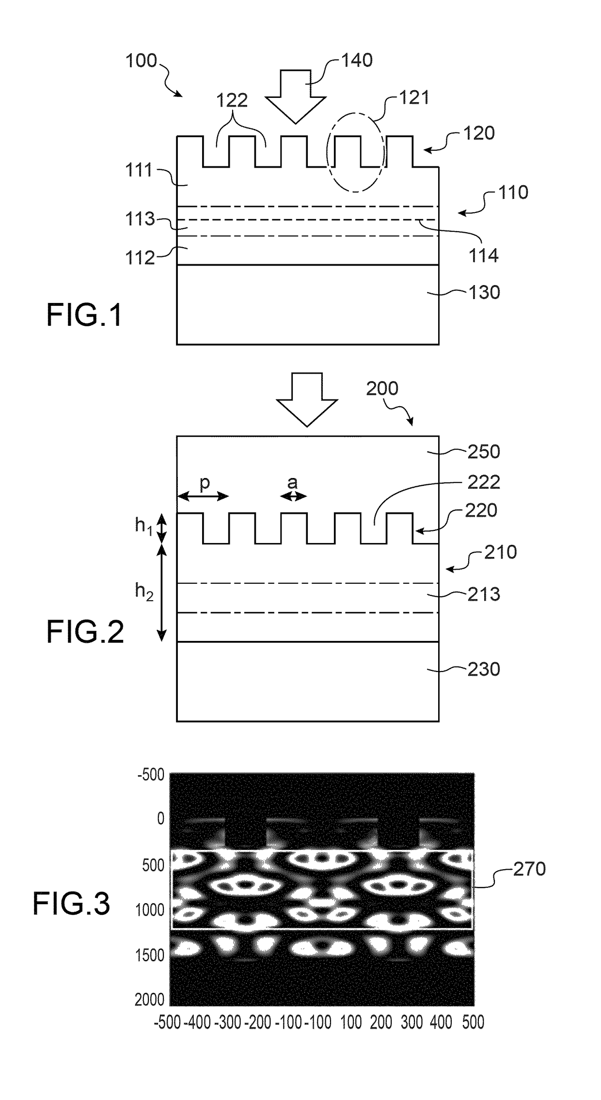
[0033]FIG. 1 schematically illustrates a photodiode according to the invention;
second embodiment
[0034]FIG. 2 schematically illustrates a photodiode according to the invention;
[0035]FIG. 3 illustrates a distribution of the absorption of light in the photodiode illustrated in FIG. 2;
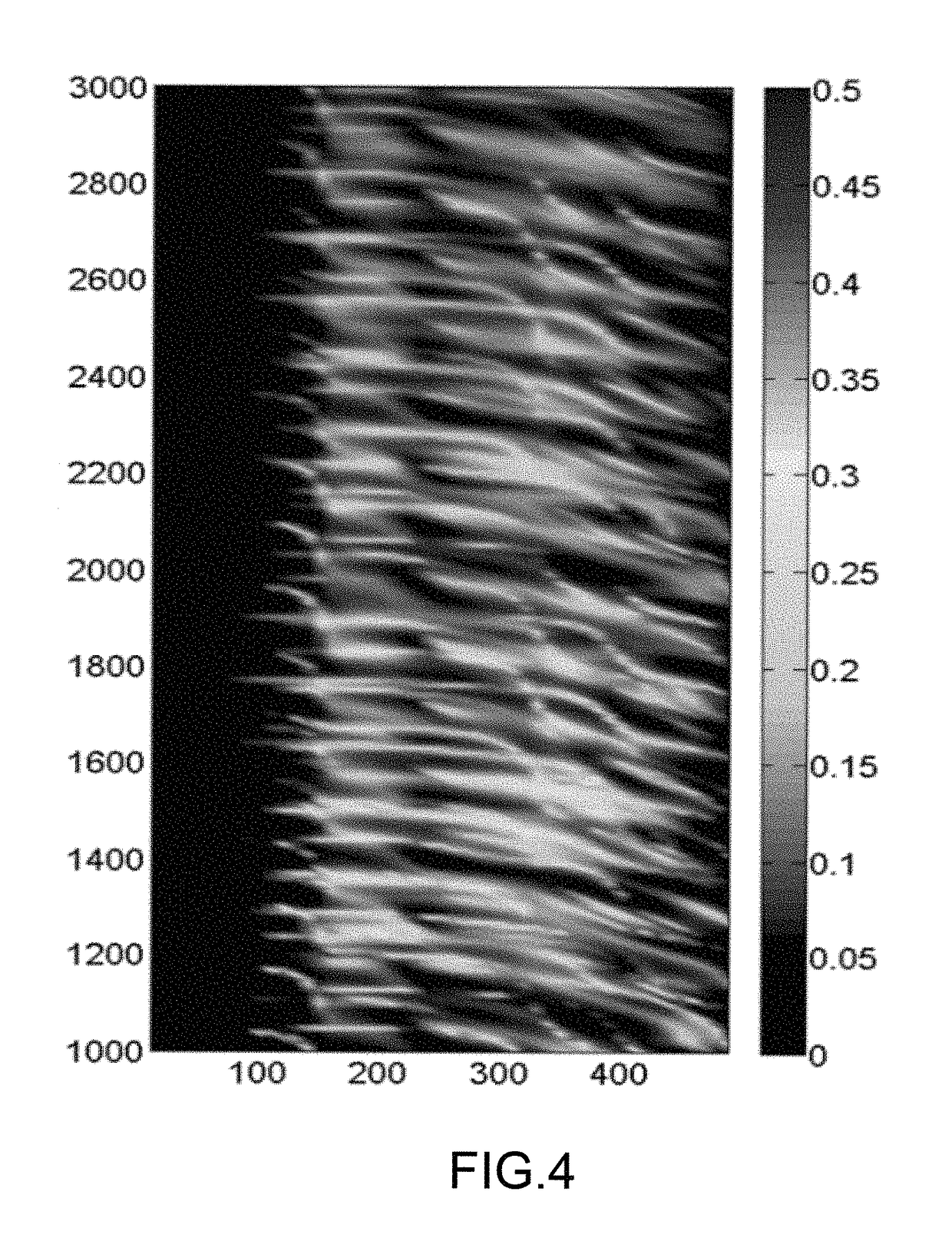
[0036]FIG. 4 illustrates the quantum efficiency in a photodiode according to the invention;
[0037]FIG. 5 illustrates a method of manufacturing an example of photodiode according to the second embodiment of the invention;
third embodiment
[0038]FIG. 6 illustrates a photodiode according to the invention;
Login to View More PUM
 Abstract
The invention relates to a single-photon avalanche diode (SPAD) photodiode having a layer made of semiconductor material, including an N doped zone and a P doped zone separated by an avalanche zone. The semiconductor material layer is intercalated between a periodic structure and a low index layer having a refractive index less than that of the semiconductor material layer and less than that of the periodic structure. The periodic structure is deposited directly on the semiconductor material layer. The photodiode provides low temporal dispersion and high quantum efficiency, without requiring a strong charge acceleration voltage.
Description
TECHNICAL FIELD[0001]The present invention relates to the field of photodiodes, in particular SPAD type photodiodes.STATE OF THE PRIOR ART[0002]A photodiode is a light sensitive component, including a layer made of semiconductor having an N doped zone (having an excess of electrons) and a P doped zone (having a deficiency of electrons). The N doped zone and the P doped zone are separated by a PN junction, at the level of which a depletion zone forms, also known as space charge zone. Each N or P doped zone is connected to an electrical connector, in order to polarise the diode. A photon absorbed by the semiconductor material layer generates an electron-hole pair, that is to say a positive electric charge and a negative electric charge.[0003]In a so-called SPAD (single-photon avalanche diode) photodiode, a reverse polarisation is applied between the N doped zone and the P doped zone. The polarisation voltage is preferably greater than (or equal to), in absolute value, the breakdown vo...
Claims
Login to View More Application Information
Patent Timeline
 Patent Type & AuthorityPatents(United States)
IPC IPC(8): H01L31/0232H01L31/107H01L27/144H01L31/18
CPCH01L31/02327H01L27/1446H01L31/107H01L31/1804
InventorFREY, LAURENTMOUSSY, NORBERT
OwnerCOMMISSARIAT A LENERGIE ATOMIQUE ET AUX ENERGIES ALTERNATIVES