High speed high voltage switching circuit

a high-voltage switching and high-speed technology, applied in logic circuits, logic circuit coupling arrangements, pulse techniques, etc., can solve the problems of high cost, complex pin/nip driver circuits, and complex gate driver circuits

Active Publication Date: 2017-09-05
RENO TECH
View PDF210 Cites 31 Cited by
  • Summary
  • Abstract
  • Description
  • Claims
  • Application Information

AI Technical Summary

Benefits of technology

[0011]FIG. 1 is a first exemplary embodiment of a high voltage control circuit shown in conjunction with power supplies a PiN / NiP diode as an exemplary electronic switch; and
[0012]FIG. 2 is a second exemplary embodiment of a high voltage control circuit.

Problems solved by technology

This condition of maintaining the high voltage MOSFET turned ‘on’ requires the circuit driving the gate to float above the source, which can be a problem since it necessitates the use of complex circuitry to drive the high voltage side MOSFET.
Gate driver circuits become even more complex when used as part of PiN / NiP diode driver circuitry, in uses when the PiN / NiP diode needs to be turned ‘ON’ or ‘OFF’ for a considerable duration.
For these reasons, PiN / NiP driver circuits are generally complex and expensive, and less complex and expensive PiN / NiP driver circuits are desirable.

Method used


Image

  • High speed high voltage switching circuit
  • High speed high voltage switching circuit
  • High speed high voltage switching circuit

Examples


Embodiment Construction

[0013]The description of illustrative embodiments according to principles of the present invention is intended to be read in connection with the accompanying drawings, which are to be considered part of the entire written description. In the description of embodiments of the invention disclosed herein, where circuits are shown and described, one of skill in the art will recognize that for the sake of clarity, not all desirable or useful peripheral circuits and / or components are shown in the figures or described in the description. Moreover, the features and benefits of the invention are illustrated by reference to the disclosed embodiments. Accordingly, the invention expressly should not be limited to such disclosed embodiments illustrating some possible non-limiting combinations of features that may exist alone or in other combinations of features; the scope of the invention being defined by the claims appended hereto.

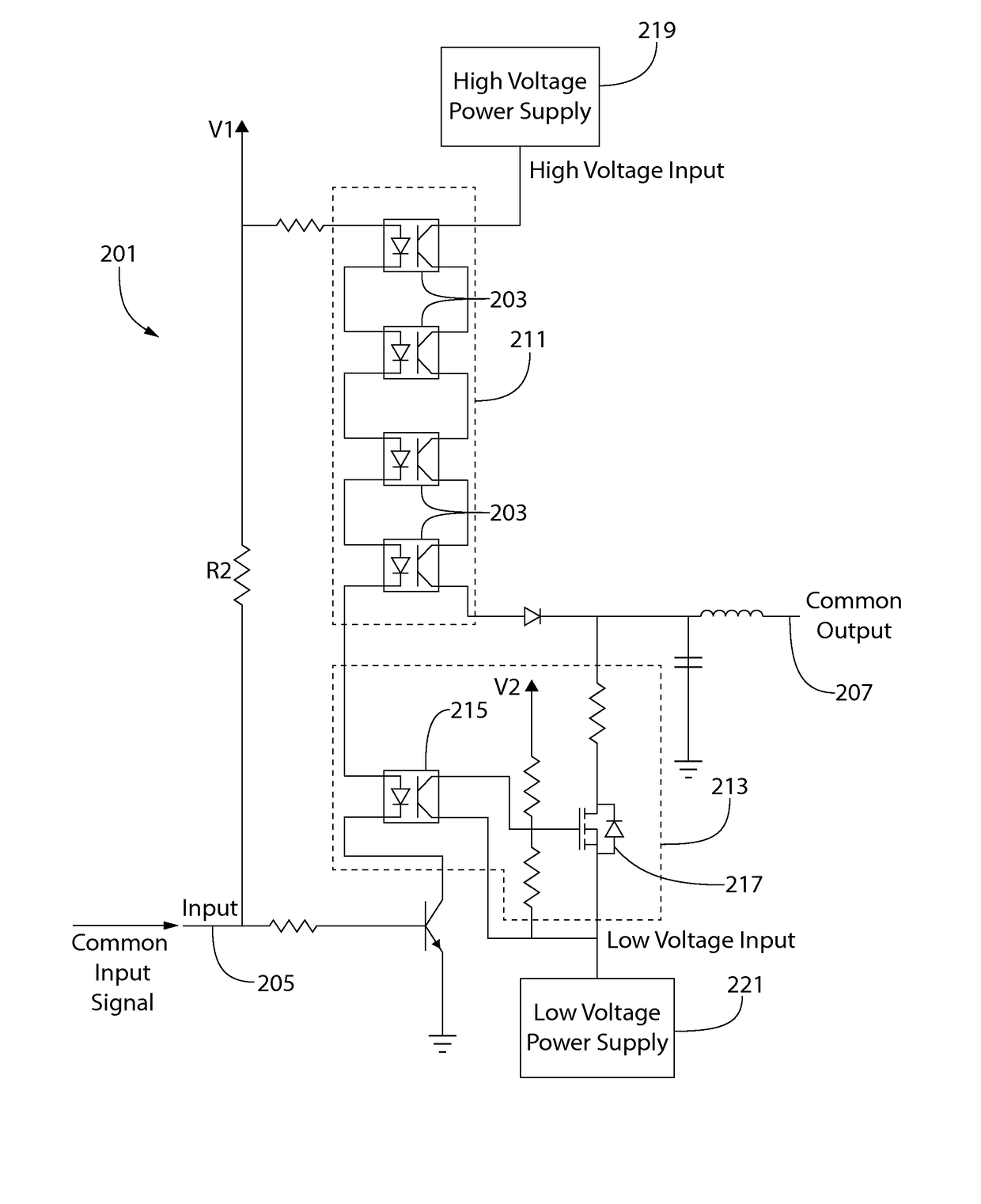
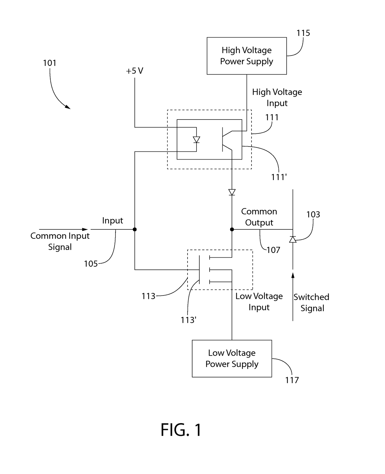
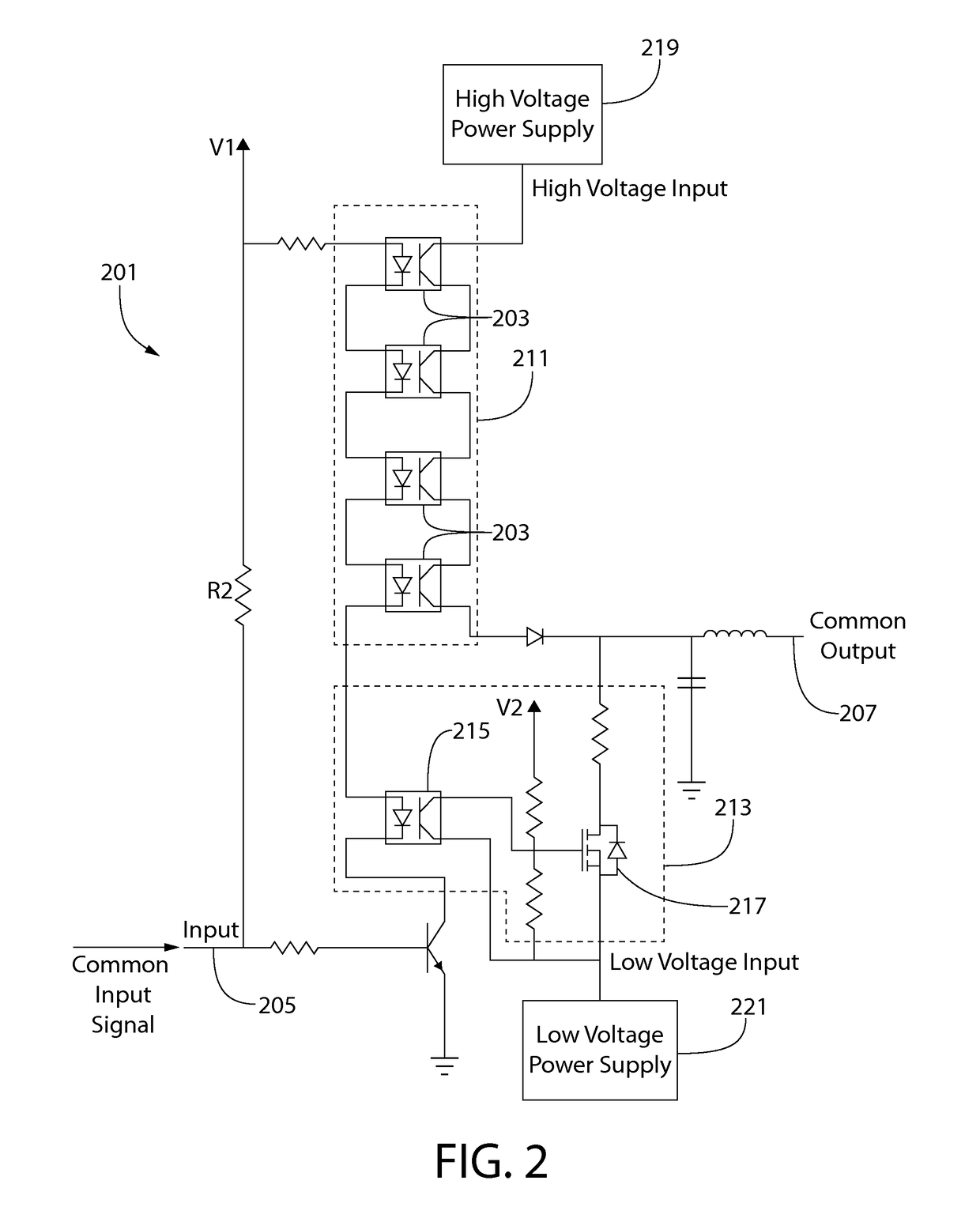
[0014]Turning in detail to the drawings, FIG. 1 shows an embodim...


PUM


Abstract

A control circuit for an electronic switch includes a first power switch receiving a common input signal and a first voltage input and a second power switch receiving the common input signal and a second voltage input. The first and second power switches switchably connect the first voltage input and the second voltage input, respectively, to a common output in response to the common input signal. The second voltage input is opposite in polarity to the first voltage input, and the first power switch and the second power switch are configured to asynchronously connect the first voltage input and the second voltage input, respectively, to the common output in response to the common input signal, the electronic switch being switched according to the first voltage input or the second voltage input being connected to the common output.

Description

CROSS REFERENCE TO RELATED APPLICATIONS[0001]Priority is claimed to U.S. Provisional Application Ser. No. 61 / 926,017, filed Jan. 10, 2014, the disclosure of which is incorporated herein by reference in its entirety.FIELD OF THE INVENTION[0002]The field of the present invention relates to electronic circuits which enable high speed switching for high voltage applications, particularly for high voltage RF applications.BACKGROUND OF THE INVENTION[0003]PiN or NiP diodes are frequently used in RF applications as RF switches. PiN / NiP diodes have the characteristic that their conduction can be changed by applying appropriate bias voltage. When used as a switch, the diode can be turned ‘OFF’ by applying a reverse bias voltage across it that is of sufficient amplitude to prevent the RF signal from passing through the diode. Similarly, a forward bias can be applied across the diode to turn it ‘ON’ and make it conduct. The current generated by the forward bias determines the amount of conducti...

Claims


Application Information

Patent Timeline
Patent Type & Authority Patents(United States)
IPC IPC(8): H03K19/017H03K19/0175H03K17/08H03K17/12H03K17/081
CPCH03K19/017536H03K19/017572H03K17/08116H03K17/08H03K17/12H03K19/017518H03K17/081H03K17/04163
Inventor BHUTTA, IMRAN AHMED
Owner RENO TECH
Why Eureka
Try Eureka